What is IC Package Design in the PCB Manufacturing Process?
By:PCBBUY 10/21/2021 09:18

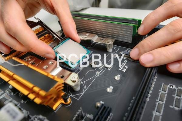
IC packaging is the last stage in the production of semiconductor devices. During this stage, the semiconductor block gets covered in a package that protects the IC from potentially damaging external elements and the corrosive effects of age. The package is essentially an encasement designed to protect the block and also to promote the electrical contacts that deliver signals to the circuit board of an electronic device.
In this article, we will focus on IC packaging design. If you are interested in IC packaging, please check and read the content below for more information.
What is the basic history of IC packaging?
IC packaging technology has evolved since the 1970s when ball grid array (BGA) packages first came into use among electronics packaging manufacturers. At the dawn of the 21st century, newer options in package technologies eclipsed pin grid array packages, namely the plastic quad flat pack and the thin small outline package. As the noughties progressed, manufacturers like Intel ushered in the era of land grid array packages.
What materials are needed in IC packaging?
The required materials used to build different IC packages are essential.
It’s because three factors establish the foundation of a package. And they are:
· Chemical properties
· Physical properties
· Electrical properties
· But that’s not all.
The performance of the package also acts as a limiting factor. So, let’s dive into the three primary package materials.
How to process the virtual prototyping of IC packaging design?
Building a digital twin, virtual model of the 2.5D/3D heterogeneous assembly provides a comprehensive representation of the full system comprising multiple devices and substrates. The digital twin enables automated verification of heterogeneous assemblies beginning with substrate-level design rule checking (DRC) and expanding into layout versus schematic (LVS), layout versus layout (LVL), parasitic extraction, stress and thermal analysis, and, finally, test.
One of the primary benefits of the digital twin approach is that it serves as the golden reference to drive complete physical and electrical verification at every level of the design hierarchy. That eliminates using multiple, static spreadsheets to represent pin and connectivity information, replacing them with a full, system-level netlist in Verilog format.

The preservation and reuse of original data, such as a device’s Verilog description, is key. The biggest risk comes when translation or conversion occurs, such as with a schematic or spreadsheet. If this is done, the “digital thread” is immediately broken, and the risk for connectivity errors skyrockets.
How to guarantee multi-domain integration?
A digital-twin methodology also enables multi-domain and cross-domain integration. Bringing more complex advanced IC packages to market faster requires highly integrated design and verification — from electronic substrate design to mechanical package heat-spreader and PCB-mounting hardware, including the interrelated aspects of electrical, thermal, test, reliability, and, of course, manufacturability. Without a system-level approach to design and verification, engineers risk experiencing costly re-spins or worse.
Synchronization of electrical and mechanical information is essential to ensuring that no physical violations occur when a package is placed within an enclosure or an entire system. The incremental exchange of data during design is fundamental to ensuring ECAD-MCAD compatibility and increased first-pass success. It also aids in the creation of more robust designs while increasing productivity and achieving faster time to market.
It is extremely important that both the IC package designer and the custom heat-spreader designer can visualize, explore, and optimize the integration, ideally as an asynchronous process that minimizes cross-domain interruptions.
What are the classifications of IC packaging?
The die of an IC is a conglomeration of interconnected transistors, resistors, capacitors, and diodes to perform specific functions. Once encapsulated in a suitable package, the internal die connects to external components via the terminals present on the package. Manufacturers like to classify different types of ICs based on the size of the die and the number of gates on it:

SSI — Small Scale Integration, containing 3-30 gates on a single chip.
MSI — Medium Scale Integration, containing 30-300 gates on a single chip.
LSI — Large Scale Integration, containing 300-3000 gates on a single chip.
VLSI — Very Large-Scale Integration, containing more than 3000 gates on a single chip.
Manufacturers also divide ICs based on the techniques they use for manufacturing them. The division follows three broad classes:
Thick and Thin film ICs: Manufacturers integrate the passive components such as resistors and capacitors, leaving out the active components. These thick and thin film ICs are usually a combination of discrete components integrated together.
Monolithic ICs: These are the most common type of ICs available today. A monolithic IC consists of discrete components, both active and passive, and the interconnections between them integrated on a single silicon chip.
Industry Category


