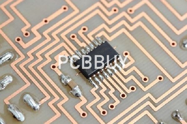
IC substrate
By:PCBBUY 07/29/2021 17:37

As one type of the most advanced PCB (Printed Circuit Board), IC substrate PCB has exploded in both popularity and applications together with any layer HDI PCB and flex-rigid PCB, now widely applied in telecommunications and electronics updates. IC substrate is a kind of substrate used to package bare IC (integrated circuit) chips, connecting chips and circuit boards.
In this passage, follow us and get into IC substrate PCB for more professional knowledge. Please check and read the content we provide for you below.
What is the divination of IC substrate of PCB?
IC substrate is a type of base board used to package bare IC (integrate circuit) chip. Connecting chip and circuit board, IC belongs to an intermediate product with the following functions:
• it captures semiconductor IC chip;
• there’s routing inside to connect chip and PCB;
• it can protect, reinforce and support IC chip, providing thermal dissipation tunnel.
What are the classifications of IC substrate of PCB?
Classified by package types
· BGA IC Substrate. This kind of IC Substrate performs well in thermal dissipation and electrical performance and can dramatically increase chip pins. Therefore, it is suitable for IC package with pin count exceeding 300.
· CSP IC Substrate. CSP is a type of single chip package with light weight and miniaturized scale, featuring similarly size with IC. CSP IC substrate is mainly used in memory products, telecommunication products and electronic products with a small number of pins.
· FC IC Substrate. FC (Flip Chip) is a type of package by flipping chip, featuring low signal interference, low circuit loss, well-performed performance and effective thermal dissipation.
· MCM IC Substrate. MCM is an abbreviated form of multi-chip module. This type of IC substrate absorbs chips with different functions into one package. As a result, the product can be an optimal solution due to its attributes including lightness, thinness, shortness and miniaturization. Naturally, since multiple chips are packaged into one package, this type of substrate doesn’t perform so well in signal interference, thermal dissipation, fine routing etc.
Classified by material attribute
· Rigid IC Substrate. It is primarily made by epoxy resin, BT resin or ABF resin. Its CTE (coefficient of thermal expansion) is approximately 13 to 17ppm/°C.
· Flex IC Substrate. It is primarily made by PI or PE resin and features CTE 13 to 27ppm/°C
· Ceramic IC Substrate. It is primarily made by ceramic materials such as Aluminium oxide, Aluminum nitride or silicon carbide. It features a relatively low CTE which is approximately 6 to 8ppm/°C

Classified by bonding technology
• Wire Bonding
• TAB (Tape Automated Bonding)
• FC Bonding
What is the application of IC substrate of PCB?
IC substrate PCBs are mainly applied on electronic products with light weight, thinness and advancing functions, such as smart phones, laptop, tablet PC and network in fields of telecommunications, medical care, industrial control, aerospace and military.
Rigid PCBs have followed through a series of innovations from multilayer PCB, traditional HDI PCBs, SLP (substrate-like PCB) to IC substrate PCBs. SLP is just a type of rigid PCBs with similar fabrication process approximately semiconductor scale.
What are the difficulties of IC substrate manufacturing?
Compared with standard PCB, IC substrate has to conquer manufacturing difficulties for its implementations of high performance and advanced functions.
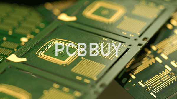
IC Substrate Manufacturing
IC substrate is thin and easy to be deformed, which is especially protruding when a board is less than 0.2mm thick. To overcome this difficulty, breakthroughs have to be made in terms of board shrinking, lamination parameters and layer positioning system so that substrate warpage and lamination thickness can be effectively controlled.
Microvia Manufacturing Technology
Microvia technology consists of the following aspects: conformal mask, laser-drilled micro blind via technology and plated copper filling technology.
· Conformal Mask aims to logically compensate laser-drilled blind via opening and blind via aperture and positions can be directly defined through copper openings.
· Laser-Drilled Microvia fabrication is correlated with the following technological aspects: via shape, aspect ratio, side etching, left gel under via etc.
· Blind Via Copper Plating is correlated with the following technological aspects: via filling capability, blind via openness, sinking, copper plating reliability etc.
Patterning and Copper Plating Technology
Patterning and copper plating technology is correlated with the following technological aspects: circuitry compensation technology and control, fine line fabrication technology, copper plating thickness uniformity control.

Solder Mask
Solder mask manufacturing for IC substrate PCB consists of via filling technology, solder mask printing technology etc. Up to now, IC substrate PCB allows less than 10um for surface height difference and surface height difference between solder mask and pad should not be over 15 um.
Surface Finish
Surface finish for IC substrate PCB should emphasize thickness uniformity and up to now, surface finish that can be accepted by IC substrate PCB includes ENIG/ENEPIG.
Inspection Capability and Product Reliability Test Technology
IC substrate PCB calls for inspection equipment that is different from that used for traditional PCB. In addition, engineers have to be available that are capable of mastering inspection skills on the special equipment.
Industry Category


