What is Included in PCB Fabrication though 5 Essential Factors?
By:PCBBUY 12/25/2021 10:29

Electronics and PCB manufacturing is presently facing several challenges together with opportunities. Along with the need to control costs, the PCB manufacturing services will have to focus on finding ways of capitalizing on current trends. This may include integrating technologies outside their primary areas of expertise, while meeting demands from customers for highly efficient manufacturing processes that are also eco-friendly.
Then what are the main factors during PCB fabrication? If you are going to learn more about PCB fabrication, please check and read the content below in this passage.
What are the 5 factors of PCB fabrication?
It might not be helpful to jump directly into fabrication without knowing the relationships and steps between the schematic or idea you have in mind and getting that idea made. Before defining PCB fabrication, it may be helpful to define a few other terms and their interrelationships.
PCB Development: PCB development can be defined as the process of taking a circuit board design from the design to the production. This typically includes three stages: design, manufacturing and testing. And for all but the simplest designs, this process is iterative with the objective of arriving at the highest quality design within the development time allotted.
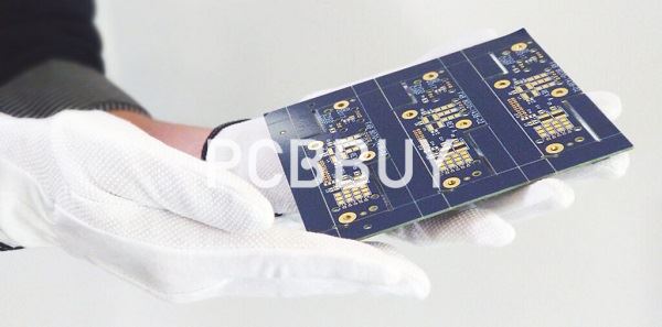
PCB Manufacturing: PCB manufacturing is the construction of your board design. This is a two-step process that begins with board fabrication and ends with printed circuit board assembly (PCBA).
PCB Testing: PCB testing, sometimes referred to as bring up, is the third stage of PCB development; performed after manufacturing. Testing during development is done to evaluate the board’s ability to perform its intended operational functionality. During this stage, any errors or areas where the design should be modified to improve performance are identified and another cycle is initiated to incorporate the design changes.
PCB Assembly: PCB assembly or PCBA is the second step or stage of PCB manufacturing in which the board components are mounted to the bare board through a soldering process.
PCB Fabrication Process
PCB fabrication is the process or procedure that transforms a circuit board design into a physical structure based upon the specifications provided in the design package. This physical manifestation is achieved through the following actions or techniques:
· Imaging desired layout on copper clad laminates
· Etching or removing excess copper from inner layers to reveal traces and pads
· Creating the PCB layer stackup by laminating (heating and pressing) board materials at high temperatures.

What are the basic PCB design rules in fabrication?
The routing guidelines for PCB design
Printed circuit board design rules and PCB layout guidelines become more complex as the number of layers in your stackup increases. Your routing strategy will require alternating horizontal and vertical traces in alternating layers unless you separate each signal layer with a reference plane. In very complex boards for specialized applications, many of the commonly-touted PCB best practices may no longer apply, and you'll need to follow PCB design guidelines that are particular to your application.
Defining net widths
Your printed circuit board design will likely require different nets that will carry a wide range of currents, which will dictate the required net width. With this basic requirement in mind, it’s recommended to provide a 0.010” width for low current analog and digital signals. Printed circuit board traces that carry more than 0.3 A should be wider. Here’s a free Trace Width Calculator that makes this process easy. You can also use this calculation (based on IPC-2152) to determine your PCB trace width.
Board constrain guidelines for PCB design
These guidelines are linked with restrictions of the overall board's shape, size, and some design aspects that influence the concept or design of the PCB. It entails selecting the reference center that benefits the PCB manufacturing process. The reason for this is to have reference points or holes on the board, which are employed for test fixtures and place and pick machines. It also helps enable enough board ground for the circuit.
In most cases, the board's dimensions are elucidated by the size of the product; however, prior to manufacturing PCB designs, the evaluation must be made concerning the board size. It will also be easy to evaluate the layers needed to develop PCB at the start of the design. If more layers are included, then the overall production cost will rise. It is yet critical to ponder how the PCB will be mounted at the start of the design.

What is the importance of PCB fabrication failure analysis?
As smart phones, tablets, and wearable devices have become smaller, thinner, and more functional, PCBs and components continue to be even smaller, denser, and more layered. In the automotive industry, research and development of technologies such as automatic brakes and autonomous driving has promoted computerized control of important components. Such control then expects PCBs and electronic components to have high durability and reliability so as to withstand long-term stress caused by driving, accelerating, and stopping.
Terminals and devices now have an important role in various daily situations, and cars require a high degree of safety. Any failures and defects of important components that are computerized in such products can lead to serious trouble or accidents.
To evaluate the durability and reliability of PCBs and electronic components, reliability evaluation tests, including acceleration tests, have become increasingly important. In addition to such tests, using microscopes to identify defects and failure causes is more important than ever.
Industry Category


