What is Manhattan Routing in PCB Manufacturing Process?
By:PCBBUY 12/01/2021 09:24

Manhattan Length is the shortest path that a wire can have when it must be connected using only segments that are confined to either the X axis or Y axis. Calculating the Manhattan Length is quite simple. One need only subtract the X coordinates of the two end points from each other and the Y coordinates of the two end points from each other and sum these two dimensions.
In this passage, we will focus on the Manhattan routing during the PCB manufacturing. If you are curious about the Manhattan routing during the PCB manufacturing, please check and read the content below for more.
What is the Manhattan routing?
Manhattan routing is a PCB routing strategy. You use one dedicated layer for horizontal tracks and another layer for vertical tracks. No horizontal tracks are allowed on the vertical layer, and no vertical traces are used on the horizontal layer. This means that most connections will go through a via, but this strategy can provide surprisingly dense boards with little routing effort. Look at a map of Manhattan: streets are straight and at right angles. That's what you do on your PCB: horizontal and vertical lines.
What are the advantages of Manhattan routing in PCB?
Manhattan-Style routing being the use of expressly east-west planes and north-south planes, using a via and changing planes when a signal changes direction. Comparing to freestyle routing, which lets define as routing signals in any direction on a given layer, would manhattan routing generally result in increased density, signal integrity, and more or less layers?
The primary advantage of a Manhattan route is that it can always be completed. You just need to have enough board area to accommodate all of the traces — but otherwise, you'll never find yourself unable to complete a route. This can be important if you need to get a layout done on a fixed schedule — the amount of work is roughly proportional to the number of pins, and you won't spend days or weeks trying to complete the task because of blockages.
Other routing algorithms might be more efficient than Manhattan in terms of board area and the number of vias required (saving money on each board produced), but they cannot guarantee completion of the route in every case, which means that there's a nonrecurring cost risk in terms of the engineering effort required.

What are the causes of Manhattan routing in PCB?
As we mentioned already, the term “Manhattan routing” is based on the regularly spaced roads in New York city that crisscross horizontally and vertically on a grid. Although we use the term to describe PCB routing, “Manhattan” is also associated with distance or length, and wiring as well.
Manhattan Distance or Length
The Manhattan distance is the shortest path that a wire can have when it is restricted to being routed orthogonally, or in the X and Y axis only. Manhattan distance becomes important when the two points being measured are not aligned in the same axis with each other. While the direct measurement of a diagonal path will be the shortest distance between the two points, the orthogonal path of following a grid pattern will be longer. Measuring Manhattan length is relatively easy by adding the X distance(s) to the Y distance(s) between the two points.
Manhattan Wiring
This is a method of laying out circuitry for an integrated circuit. The interconnects are aligned with a grid, and the connection points are perpendicularly creating a Manhattan pattern. This method of representing circuitry can be done either physically in the chip, in the documentation, or in both. There are also other terms for Manhattan wiring such as right-angle wiring, and they are all based on what is known as the taxicab geometry. This description again goes back to the idea of traveling in gridded orthogonal movements in order to get from one point to another in a city like Manhattan.
What are the techniques of Manhattan routing in PCB?
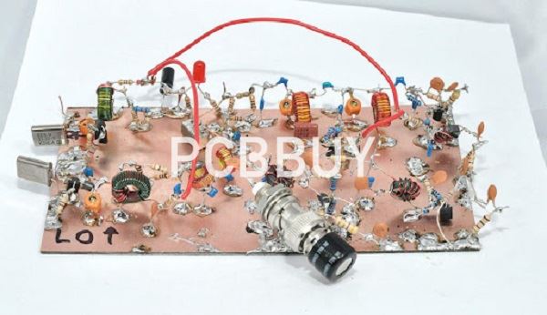
One really neat method of building circuits without making a PCB is called Manhattan style, so called because the components look like buildings in Manhattan. I really like it because it’s simple, quick, and if you do it right, can be good enough for RF frequencies. I also like the way it looks. The method I’ve been using is to get free samples of Rogers material, most of which can be cut with just scissors. It’s a little easier than scoring and breaking FR4, but the trade off is that the copper clad board can bend slightly, which can crack some of your joints. You use the main copper surface as a ground plane, and superglue small squares of copper to use as nodes. Here are a couple of the circuits I’ve built using this style:

With a set of advanced PCB layout tools, you can set up a number of different design constraints to control the direction of your trace routing, plus much more. You will also have features in the tools that will assist you in your routing by reporting trace lengths and other useful data. In the picture above you can see how these tools have reported the direct distance, the Manhattan distance, and the actual etch distance of the selected trace routing. In this case, the actual trace routing is slightly less than the Manhattan distance due to its more direct routing pattern.
The PCB design system that you need for Manhattan routing and other advanced PCB layout tasks is from Cadence. OrCAD PCB Designer has the features and functionality that you need to configure your design rules and constraints before you route, as well as reporting back to you the status of your routing as you work.
Industry Category


