What is PCB Assembly Process in Factory?
By:PCBBUY 08/16/2022 16:38

Do you know the process of PCB assembly after manufacturing in a factory? If you are curious about the PCB assembly process, please check and read the content in this passage for more information.

What is the importance of PCB design for assembly?
When it comes to anything you do—whether it’s cutting the grass or cooking a meal—we usually want the end result to turn out the way we planned. The same can be said when designing a PCB—we should worry first about getting it to work first, right? The answer here is both yes and no.
Not only do we need our PCBs to work the way that we’ve designed them too, but those boards must be manufacturable for a reasonable price as well. There are several factors that can contribute to a board not being considered manufacturable. Here are the main categories of problems:
Components
Parts that are unique or not readily available will have higher costs attached to them. Also if the lead times on some parts cause delays in the board build, that will add to the expense as well.
Placement
How you place your parts can affect how the board is manufactured and drive up costs. Even simple things such as how a component is rotated can affect its solderability.
Layout
Your PCB design will usually connect to other boards or interfaces. If these considerations haven’t been accounted for up front, it could add to the expense of manufacturing the entire system.
How to solve common problems during PCB assembly?
Plated through holes are important holes on the printed circuit board, as they carry electricity from one side of the board to the other side through the holes. The walls of these holes are electroplated during the PCB fabrication process. Before electroplating, the circuit board is made conductive from the top to bottom by copper deposition.
In this process, the electroless copper is made to adhere to the edges of the circuit board and within the holes. The problems with copper deposition give rise to plating voids, which means the walls are not coated evenly with copper. These holes may affect the flow of electricity. Plating voids may be caused due to a variety of reasons such as material contamination, air bubbles in the material, contaminated holes, and so on. So, the defects caused due to air bubbles, contamination, and insufficient cleaning can be avoided by cleaning the material before drilling. Also, other defects can be avoided by following the directions provided by the manufacturer.
Failure of PCB is linked to physical damage, which is caused due to environmental stresses or during the SMT manufacturing process. Most common cause of PCB failure is dropping a circuit board in a prototyping phase. The damage to the physical components or pieces is not easily visible, and they are not repairable either. Thus, there is no other option except replacing the PCB.
What is the process of PCB assembly?
Solder Paste: If you’re following a traditional PCB assembly process, the first step is the application of solder paste. Note that this is not the case with THT, but SMT does require paste application and/or printing.
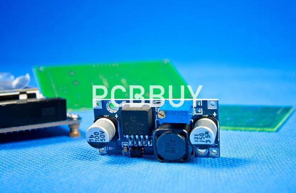
Component Placement: In the traditional PCB assembly process, the next step is to place the components on the board. This can be done manually, or it can be done with the assistance of machinery (pick and place systems). In THT assembly, components are placed by hand, which requires incredible precision. In the SMT process, robotic systems place components on the board. Note that automated placement is far faster than manual placement and is just as precise.
Reflow: In the traditional PCB assembly process, the next step is reflow, which is when the solder is first melted and then resolidified. The board and all its components move through an oven, which heats the solder, liquifying it and ensuring that connections are formed before the board moves into a cooler, where the solder is cooled.
Note that the THT process does not require reflowing solder. Instead, the second step here is to inspect the board and rectify component placement. This is due to the manual placement process – a visual inspection in conjunction with a design transport frame helps ensure placement accuracy.
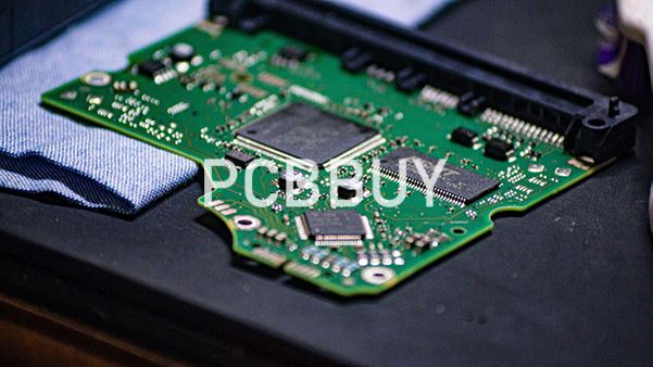
In the SMT process, reflow soldering takes place at this time, as well. The board is sent through a furnace, which melts the solder paste, allowing it to flow as necessary, before the board passes through a series of coolers that gradually bring the temperature down, solidifying the solder on the board and cementing the components in place.
Inspection: The next step in the traditional PCB assembly process is a visual inspection of the board, soldering, and components. Note that this step has already occurred in the THT and SMT processes.
Through-Hole Part Insertion: The traditional process requires that through-hole insertion be done manually, after the reflow and inspection process. Soldering is also often done manually, but it may be done using wave soldering.
Wave soldering occurs during the THT process at this point, as well. The entire board moves over liquid solder and then moves through coolers to solidify the solder.
Industry Category


