What is PCB DFM during the PCB Assembly Manufacturing Process?
By:PCBBUY 11/18/2021 09:50

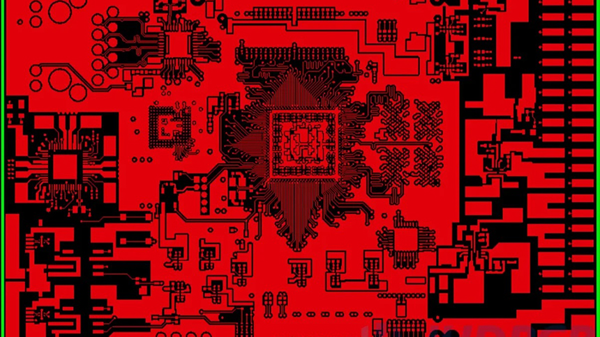
DFM analysis software can help solve these problems. The term DFM stands for Design for Manufacturability. This process compiles PCB layout topology to reduce problems that can be encountered during the PCB fabrication and assembly processes required to manufacture an electronic system. Without DFM analysis software, determining if the problem is manufacturing or design related becomes an expensive guessing game.
In this passage, we are going to learn more about PCB DFM. If you are interested in the PCB DFM, please check and read the content below for more information.

How to choose material for PCB DFM?
Below are the parameters that should be considered while choosing materials that meet the design criteria:
· Moisture absorption
· Fire retarding
· Electrical properties
· Mechanical properties
· Thermal properties
See our post, how to choose PCB materials and laminates for fabrication to gain a better understanding of material characteristics and selection attributes.
Why DFM is important to PCB design?
Often design teams look at DFM as a “manufacturing problem” and something handled by their contract manufacturers or downstream partners. In fact, many manufacturers will perform DFM analysis prior to production to identify and fix issues. Where this process tends to fall apart is manufacturers often do not share any changes they made back to the design team and changes made are done without a full understanding of the design and its performance / electrical requirements.
The results can be devastating when a design team then sends what they think is the spec for the previously manufactured board off for a new rev, a new production line, or second source partner and soon realizes the PCB fails in some, most, or all of the finished devices. Performing your own analysis prior to the prototype could have detected those same issues and altered them in engineering, allowing you to incorporate the changes into the PCB design where they belong. Doing so would have lowered the cost, maintained design intent, and ensured follow-on builds also work correctly.

What is the purpose of PCB DFM design?
The purpose of DFM is to eliminate the once-common miscommunication between designers and manufacturers. In past decades, the two parties would often come into conflict due to mutual misunderstandings. In a typical scenario, the designer would conceive a product with a set of measurements and a list of materials. The designer would then send the blueprint and sketches to the manufacturer, whose task was to put the design into production. If they found any problems in the design, the designer would leave it to the manufacturer to rectify these issues.
From the designer’s point of view, the steps that occurred after the design stage, including modifications, were the manufacturer’s responsibility. The trouble is that the manufacturer would usually not understand the intricacies of the design process, but would know when certain measurements or materials were either impractical or impossible. In cases like these, productions sometimes got delayed for last-minute design overhauls that would often be costly for the parties involved. Sometimes, manufacturers rushed the designs to production anyway, despite the flaws and the risk of product defects and customer dissatisfaction.
With DFM engineering, specialists from all stages in the design, development and production processes work together along every step of the way. Together, they form a combined team where engineers from each department hear the other’s input and feedback in real time as products get developed, tested and sent back for revisions. DFM saves money and time by helping companies catch design flaws almost immediately and rectify them long before the manufacturing team commences with production.
How to check PCB DFM during manufacturing?
When your contract manufacturer first receives your design data, it should go into a thorough design review. How the data is processed by the CM will be determined by what format you choose to send it in.

Data that is received in a PCB design CAD database format will go directly into engineering for review. Data that is received in other formats must be imported or translated into the tools that the CM is using. This process takes longer and is less reliable, which is why your CM would rather get the original CAD database instead. Also, if the CM ends up making any design changes, they can do that in the original data format much easier as well.
The component engineers at the CM will review your bill of materials, looking for parts that are not recommended for manufacturing, have long lead times, or are going end of life (EOL). At the same time, the design engineers at your CM should be reviewing your data for DFM issues, including signal integrity, manufacturability, and testability.
Industry Category


