What is PCB Electrical Testing during the Manufacturing Process?
By:PCBBUY 01/19/2022 09:45

Like how electricians check for a range of electrical functions in commercial and residential electrical wiring, circuit boards also undergo this process. However, the type and manner slightly differ. Nonetheless, the endgame often proves similar – to ensure the integrity and proper functioning of the circuitry.
In this passage, we are providing all the details about the PCB electrical testing. If you are curious about PCB electrical testing, please check and read the content below for more professional knowledge.
What are the main types of PCB electrical testing?
There is no specific test required for electrical testing of PCBs, as long as whatever tests performed prove the board meets electrical testing standards. Electrical testing procedures for printed circuit boards can include:
Capacitance Testing
This is a type of testing that looks for shorts in the board. The process involves charging a net with electricity and then measuring the induced capacity.
Resistance Testing
This type of testing measures resistance in ohms. The resistance is a measure of the collisions that occur between electrons and atoms that can disturb electron flow when current flows through the conductor. When testing for resistance, you are looking for low resistance as an indicator of a good conductor. Circuits have more resistance the longer and thinner they are, so this is a consideration you must take into account when testing.
Comparative Testing
This is done using a standard master board that you have already verified to teach a net list program, which you then compare your other boards against. The problem with this type of testing is that there is always the possibility the master board had an initial defect.
Continuity Testing
This test ensures the resistance between test points does not exceed the required limits.
Flip Test
Testing is done on either side of the board as a universal grid. It’s much less accurate than the clamshell method below.
Clamshell Testing
Simultaneous testing of both sides of the board are done at once. This method is a popular method for reliability, as you are testing all points on the board at once.
Adjacency Testing
Testing for shorts is conducted by checking isolation between conductors. You can test for proximity adjacency or line-of-sight adjacency.
Adjacency Test
This test checks isolation between conductors.
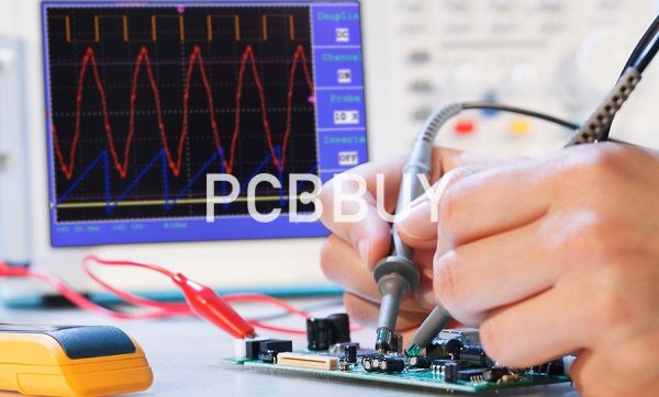
Flying Probe Testing
This very reliable method of testing involves the use of a flying-probe test sequence, which probes the board at high speeds looking for shorts and openings throughout the board.

When to process PCB electrical testing during manufacturing?
Once the part has completed processing and is in its final ship format, single pieces, or array layout, some ship in a larger panel form, the final product is electrically tested. Often ET is not considered at all by designer or even by PCB manufacturers. Why is this? Well, there are several reasons. With technology increasing, layer count, blind vias, components all add time. Each electrical connection has a start and end point. Some circuits jump from layer to layer using vias as their passageway to the end point. Mid-points in circuitry are plenty full as well as test points (TP) that are placed for end-product testing once assembled. All the examples must be tested, the more there are the longer the test can take.
We estimate the ET time using only what we know, quantity of vias, single sided, or double-sided component placement, the number of through holes, blind holes, or buried holes. From these numbers, we can only calculate what we believe the test time will be.
Testing equipment varies. In most facilities, the flying probe, bed of nails, or clam shell are commonly in place. Bed of nails testers are the traditional or original testing method. Using a bed of nails tester requires a customer build fixture containing, plexiglass layers, standoff pins, holes drilled through the layers to support pogo pins. Typically, a known good board that has passed is kept with the fixture to test the parts against. The area needed to store the fixture is a problem, the fixtures are not small and take up valuable space but are necessary to keep. This is not the desired test method for higher technology today, but it is still used.
Flying probe or probe-bot testing is an electronic method of testing and is the most widely used in most facilities today, more reliable, and takes up less space, however, it is a much slower process. Yes, slower, but fascinating to watch. As each probe arm moves quickly from point to point to test the part, it can take a few minutes to complete the single piece test; we have recorded more than 45 minutes per piece to test a part.
Industry Category


