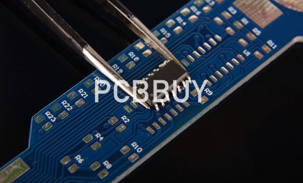
PCB Footprints
By:PCBBUY 08/30/2021 09:49

PCB footprints is very important process to PCB, There's more that goes into your PCB footprint checklist than the locations of pads on your components. Courtyard areas, component designators, and more are encoded in your component model and will appear directly on the PCB layout once you place a footprint.
The PCB footprint is defined as the physical interface among electronic components or land pattern and printed circuit boards which also comprises of the information of documentation such as reference, polarization mark, and outline.
In this passage, we will tell you everything about PCB footprint knowledge, and if you are going to learn more about it, please check and read the content below for more information.
What are considerations of PCB footprint?
Every component that will appear on a circuit board layout will have a PCB footprint. Whenever you start a new project and jump into a layout, schematic symbols and PCB footprints need to be correct before a single design document is created.
Every PCB footprint will contain the following elements:
Pad or hole locations
This shows where mounting pads (for SMD components) or mounting holes (through-hole components) are located. These locations are used for soldering and must be designed accurately.
Courtyard and outline
This act like a keepout area in your PCB footprint, i.e., other components cannot be placed within the PCB footprint courtyard.
Reference designator
This alphanumeric code provides a unique identifier of the component in your schematic and PCB layout.
Pin-1 designator
Some components may have arbitrary orientation (e.g., QFP and DIP components). The pin-1 designator tells the assembler the correct orientation.
Mechanicals
Some components may have some mechanical element or overhang that might extend above a component and create a collision with other components. One example is a heat sink, which does not have an electrical connection to the PCB quote. These can be defined in a mechanical layer in your PCB layout.
Link to 3D model and symbols
Every PCB footprint has a corresponding schematic symbol, and it may need a 3D model. This lets you visualize the board in 3D and enables 3D clearance checking between components.

What are the guidelines of PCB footprint?
Components are the most important elements of the board, and pads are the points of connection. If the pad layout fails to accurately identify your component locations or isn’t arranged such that the component can be securely attached, the PCB cannot be assembled. If the pads don’t line up properly with other surface elements like traces and drill holes, your board will not function properly or at all.
Foot print pad layout
Footprint pad guidelines are rules or suggestions that stipulate how pads should be spaced from other pads, other surface elements, drill holes and the board edge. They also define how pads for a single component should be arranged.
Start with exact information
Ensure that you have the correct specifications for the part and the relevant standards, such as IPC-7351, to use as a blueprint.

Build the footprint from the ground up
Start first with the pad information. Whether your tools require a separate pad part, or you must add the pad geometry as an attribute, ensure you have what you need first. Next, create the body outline of the component at the maximum material width. Finally, add silkscreen outlines, reference designators, other attributes, and STEP models to finish the footprint.
Make sure to include all the required data
Often a footprint is left incomplete, which can cause problems during PCB layout. For instance, if your CAD tools require you to enter the part’s height as an attribute, don’t neglect this. Later on, you may wonder why you didn’t get a warning when you find out that your component is sticking up through the device enclosure.
Be cautious of including too much data
Do your footprints need drawing formats, mechanical data, and dimensions? Remember that each footprint will be replicated for each instance of that part in the layout. If you have included all of this extra data, it will also be replicated. Viewing the CAD layer designated for footprint dimensions will result in a confusion of jumbled data that can be difficult to discern for assembly.
Industry Category


