What is PCB Lamination through 5 Essential Factors?
By:PCBBUY 11/09/2021 09:32

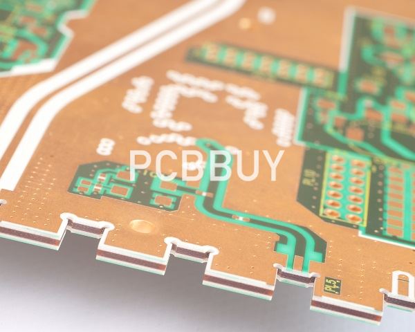
A printed circuit board is a structure used to connect and support electronic components, which are made up of laminate including mostly glass epoxy base material with coating of copper on single or either side of it. And the boards have conductive pathways through which different components are connected across the board. These pathways are etched from copper sheets. To ensure that the copper layer does not conduct a signal or current, it is laminated into a substrate.
However the lamination requirements of various kinds of printed circuit boards depend upon their nature, type and the area of use. Are you going to learn more about PCB lamination? If you are curious about PCB lamination, please check and read the content below.
1. What are the types of PCB lamination?
The PCB lamination process occurs at the point in fabrication when the inner layers, foil and prepreg are stacked, heated and pressed into a circuit board. As with many processes in circuit board fabrication, method and materials vary.
· A multilayer PCBA is fabricated in various layers, either as thin-etched boards or trace layers that are then bonded with lamination. In this standard process, internal layers are heated intensely and put under pressure prior to high-temperature curing. As the PCB slowly cools, pressure is released before the circuit is laminated with a photosensitive dry resist.
· Teflon (PTFE) microwave laminates are commonly used for RF circuit boards with high-speed signal flows. Characteristics like minimal electrical loss, tight depth tolerance, and a reliable dielectric constant, make them ideal PCBAs for applications involving radio frequencies.
· Sequential lamination is a popular method when a PCB has two or more subsets. After creating subsets of multi-layered PCBs in a separate process, with an insulating material between each pair, standard PCB lamination processes are then implemented. It should be noted that this method adds time and cost to the build process.
2. How to process PCB lamination?
Lamination is the point in the PCB fabrication process where all of the inner layers, prepreg and foil are assembled into a stack that is pressed and heated to create the final multilayer PCB.
There are two ways to laminate a PCB. They include:
· Foil lamination
· Cap lamination
3. What is the importance of PCB Lamination?
High-density interconnects (HDI) PCBs are a rapidly increasing part of printed circuit boards (PCBs) and electronics industries. To achieve higher circuit density than traditional PCBs, HDI printed circuit boards utilize a combination of advanced features and technologies such as blind/ buried vias, laser-drilled stacked micro-vias, via-in-pads techniques, among others. One of the most crucial manufacturing techniques in the HDI PCB fabrication process is Sequential Lamination.

4. What is thermal stress of PCB Lamination?
One other area the CTE of PCB can affect the reliability of the PCB assembly is in thermal stress cracking of the via copper plating, with repeated thermal cycles. The expansion of PCB materials is volumetric by temperature rise, however the laminate construction is such that x-y expansion, and z-axis are significantly different.
The restraining glass fabric in the laminate, prevents the resin from expanding isotropically (the same amount in all directions) therefore the x, y expansion will be significantly less than the z axis
The resin volume expansion, (glass does not expand by much) is controlled by the high young’s modulus (strength of the expansion force) of the stronger glass laminated within the x-y circuit layers. This simply means that the resin is restricted from moving in the x-y axis by the lower expansion rate of the glass laminate, therefore it must expand in the z axis. Unfortunately, this means that the resin will expand significantly more in the unconstrained z axis and will apply stress to the plated copper in the vias.
5. What is the traditional PCB Lamination?
Nowadays, multilayer PCB used most of the time. This type of board is tinier in size. The component also used in the time of manufacturing concise the density of the product. In a simple word, multiple layers of circuit boards make Assembly manageable to use flexibly.
Simultaneously, PCB’s stuck-up design is a single-layer circuit board that needed some convenient fabrication. By knowing the manufacturing competence well, it will be easy to do that. Sequential lamination is a common step in the PCB fabrication process. The process is described below:
Sequential lamination’s success rate in multiple-layer boards is very high. Especially in high-density electronic technology, it is more fruitful. Here it’s the main function to maintain high signal messages like communication.
Industry Category


