PCB Library
By:PCBBUY 09/08/2021 09:26

There are many technologies during the manufacturing process. By taking the time to review your designs before you create your layouts, you can resolve issues early enough to lower costs and production time. In order to understand what a good PCB library administrator can do for you, you need to know what they can't do, as well.
When laying out printed circuit boards, we can fall victim to the same problem with our library parts. Many PCB design workflows rely on designers building their own component footprints for each layout. This is an important skill to have, but you will find yourself wasting a lot of time if you recreate the same parts over and over again for each job. If you are going to learn more information PCB library, check and read the content below.
What is the importance of PCB library?
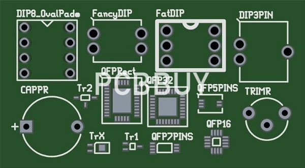
When designing a PCB, each electronic component requires a symbol for the schematic capture, which describes pin functions, mappings and types, and a PCB footprint, to ensure that the component is soldered to the board correctly. Additionally, 3D models are also generally used by engineers to check clearances between their PCBs and their mechanical casings.
High-quality libraries can be difficult to get right, but are an essential element of the PCB design process, because they ensure:
· Proper and reliable manufacturing
· Other CAD tool features function properly (ex: ERC and DRC checks)
· Consistency, which makes designs readable and reusable
Building a good PCB library comes with a number of challenges and difficulties, as discussed in Natasha Baker’s presentation. First of all, it’s a very detail-oriented process, where a high level of precision is necessary for each pin, pad, and part. Additionally, there is a lack of consistency in how datasheets are created, which can inadvertent errors during their interpretation.
Lack of standards and industry alignment is another major challenge in building high-quality PCB libraries. Additionally, users or companies have specific preferences or requirements. Up until recently, most companies had their own standards, but nowadays we’re observing a shift in the industry towards creating and using more industry standards.
Finally, a library’s importance is often underestimated and overlooked. All companies know it is important to have footprints that manufacture well, but in practice, prioritizing library maintenance over other critical tasks can be challenging.

What are the features of PCB library?
Generally, a PCB library comprises some PCB footprints that typify both physical pad collections with some mechanical characteristics of the element or unit. One can selectively pick the PCB library he wants to incorporate into his design techniques. The reason one can pick from the PCB library is because there are different types.
Different library strategies always meet different client exigencies. The PCB library requires that you understand how it works. One may get it all wrong if proper care is not taken. With the wrong PCB library set up, your PCB layout methods may fail you.
The PCB library always needs factual or confirmed schematic segment ensign or totem. Also, it requires footprints that are quality so as to block weak or deficient fragments from landing on the production chains. One can know of these deficiencies via visual exploration. The footprints are important components of your PCB library.
The kinds of sections an engineer selects in the course of designing matter so much. Various vendors come with several solutions when it comes to the PCB library. However, each tool that one uses differs based on the client. Different users have what is best suitable for them. Users should know that the moment your PCB library is perky, your panel unavoidably becomes thronged with details relating to the composite footprints of your library.
What are the different types of PCB library?
There are different ways that PCB footprints can be organized in libraries that are external to the individual design databases:

Use
These libraries are usually areas in a user’s personal account that have been set up to store component footprints, board outlines, and other design data. In some cases, they may be tied to the main library system, but usually, they are simply a “bucket” for a user to throw footprint models into.
The advantages are that a user library is under the control of the individual designer without any bureaucracy. This makes for a very fast and efficient library system where the user can save and edit model files as needed.
Project
Many corporations will split off their libraries by projects. This becomes useful when the same part needs different sized footprints between projects due to different manufacturing methods. Project libraries are also helpful for storing project-specific data such as layer stackups for specific designs. These libraries are usually monitored and maintained by a CAD librarian to ensure quality.
The advantage of this library is being able to select the correct version of a part for a specific design. For instance, boards that are built for RF designs sometimes have footprints that are slightly smaller for high-speed signals even though there are trade-offs in manufacturing. With a project library, the user can choose an RF version of a part that might be configured differently than the standard version.
Corporate
This is the main or “master” library in a company that is used for PCB design. The footprint models in this library are usually closely monitored by the company librarian, and there is an elaborate method of checking and validating them before they are available for the designers to use.
Industry Category


