What is PCB Stencil with 7 Essential Aspects in PCB Manufacturing Process?
By:PCBBUY 11/01/2021 10:37

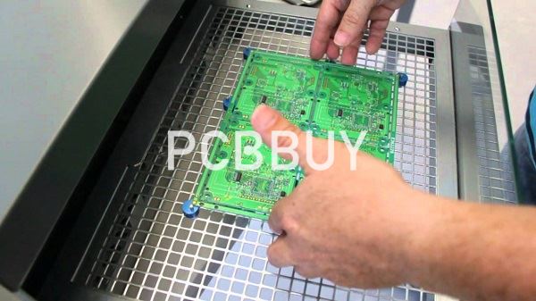
PCB Stencils are manufactured by creating openings through lasers on a stainless steel foil based sheet at the positions where Surface Mount components need to be placed on the board. The stencil is then placed on the top of the PCB and aligned perfectly using positioning points called fiducial marks. After alignment, the solder paste is applied with a metal squeegee blade. As a result of this, the solder paste gets applied to the PCB board where the surface mount components need to be placed. So when the stencil is removed, components can be placed on the board.
In this passage, we are going to learn more about the knowledge please check and read the content for more professional information.
1. How to process the PCB stencil design?
The thickness of the stencil determines the amount of solder paste printed on the PCB. Too much solder paste will cause bridging during reflow soldering. Therefore, it is recommended that the 0.5mm pitch QFN package use a 0.12mm thick steel mesh, and the 0.65mm pitch QFN package use a 0.15mm thick steel mesh. The size of the stencil opening can be appropriately smaller than that of the pad to reduce the occurrence of solder bridging.
When the exposed pads on the bottom of the chip are soldered to the thermal pads on the PCB, the gas in the thermal vias and large-size pads will overflow outwards, resulting in certain air holes. Therefore, if the solder paste area is too large, it will produce various defects (such as sputtering and solder balls, etc.). However, it is almost impossible to eliminate these pores;it is possible only to minimize the pores. When designing the stencil in the thermal pad area,careful consideration is needed.
2. Why PCB stencil is important?
Before you can go into production, solder paste is printed onto the component pads of the PCB. How can you make sure you apply the solder paste with precision exactly where it needs to go? Stencils, or formally surface mount technology stencils, are the answer. Stencils are the medium used to transfer that solder paste onto the PCB.

Stencils consist of a foil made of stainless steel that is laser cut to match the places where surface mount devices will go on the board. Once you have the cut stencil, solder paste is applied over the openings with a metal squeegee blade. When the stainless-steel foil of the stencil is pulled away, it leaves the solder paste perfectly placed on the board to receive your surface-mounted devices.
3. What is the thickness of PCB stencil?
The combination of pad size, aperture formation, and thickness determines the paste-deposition capacity of the stencil. However, even if the aperture formation and the pad size are appropriate, optimal paste deposition is impossible without the right stencil thickness.
4. How to choose PCB stencil thickness?
The thickness determines the quantity and height of the solder paste that forms a solder joint. The lower the amount, the higher the possibility of disconnects and the lower the possibility of jumpers. This correlation, called aspect results from the differences in forces acting on the paste as it glides through the aperture. These include the force that pushes the paste beyond the opening and holds the paste within the gaps.
The contrast between these two forces is represented by a measurement known as the Aspect Ratio. To achieve optimal paste deposition, you need to ensure that the Aspect Ratio is more significant than one.
5. What are the applications of PCB stencil?
SMT method provides several advantages over liquid-solder method: reduced time of production; increased production capacity; increased density of components that can be mounted onto a PCB; reducing needed design surface area of a PCB to produce a more compact product.
The sole purpose of an SMT stencil is to transfer solder paste to a bare circuit board.A well designed stencil can help to prevent 60% to 70% of SMT solder defects through the soldering process. The three commonly-occurring stencil printing defects include the following: misaligned print; erroneous stencil printing due to improper printing parameters; misalignment between PCB fiducial vs. stencil fiducial.
6. How to prototype PCB stencil?
· Precise manual SMT stencil: Alternative to hand soldering reduces the potential for errors.
· Specifically designed to manually print solder paste onto printed circuit boards.
· Eliminates tedious hand soldering of prototype circuit boards
· Reduced prototype assembly time: Quick alignment and printing increase efficiency.
· Eliminated need to use a machine: Hand-printing application requires no machine setup.
· Ultimate cost-effectiveness: Efficient design results in affordable price.
· Ease of use: Alignment tools allow for an easy-to-understand printing process.
· Allow quick alignment for repeatability

7. What are the features of frameless PCB stencil?
· Reduced storage space requirements
· Significantly less expensive than framed stencils
· Use of fewer materials suits eco-friendly production methods.
· Excellent for prototype Printed Circuit Board Assembly or short runs
· Smooth aperture walls, can be used for 16 Mil pitch and below and for Micro BGA’s
· Compatible with screen printing and hand-printing: Versatile format allows for printing with a machine or squeegee.
· 24-hour turnaround standard
Industry Category


