What is PCB assembly process?
By:PCBBUY 07/26/2021 17:06

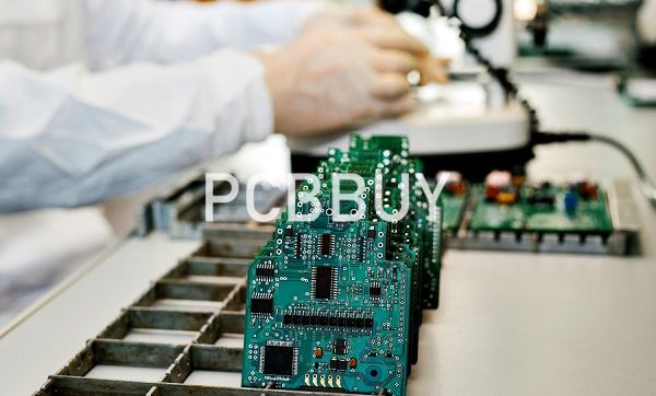
Have you ever observed those boards with components solidly stuck on? Never regard them as just decorations of a PCB board. An advanced circuit board won't be able to give its functionality until components are mounted on it. A PCB with components mounted on is called an assembled PCB and the manufacturing process is called PCB assembly or PCBA for short.
In this passage, we are going to tell you about the process of PCB assembly. Please check and read the content we provide below to learn more professional knowledge.

What is the process of PCB assembly?
Step 1: Solder Paste Stenciling
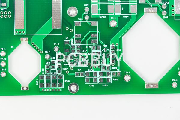
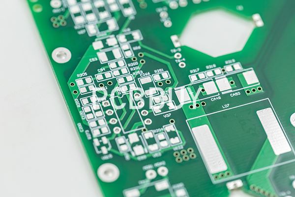
The first step of PCB assembly is applying a solder paste to the board. This process is like screen-printing a shirt, except instead of a mask, a thin, stainless-steel stencil is placed over the PCB. This allows assemblers to apply solder paste only to certain parts of the would-be PCB. These parts are where components will sit in the finished PCB.
The solder paste itself is a greyish substance consisting of tiny balls of metal, also known as solder. The composition of these tiny metal balls is 96.5% tin, 3% silver and 0.5% copper. The solder paste mixes solder with a flux, which is a chemical designed help the solder melt and bond to a surface. Solder paste appears as a grey paste and must be applied to the board at exactly the right places and in precisely the right amounts.
In a professional PCBA line, a mechanical fixture holds the PCB and solder stencil in place. An applicator then places solder paste on the intended areas in precise amounts. The machine then spreads the paste across the stencil, applying it evenly to every open area. After removing the stencil, the solder paste remains in the intended locations.
Step 2: Pick and Place
After applying the solder paste to the PCB board, the PCBA process moves on to the pick and place machine, a robotic device places surface mount components, or SMDs, on a prepared PCB. SMDs account for most non-connector components on PCBs today. These SMDs are then soldered on to the surface of the board in the next step of PCBA process.
Traditionally, this was a manual process done with a pair of tweezers, in which assemblers had to pick and place components by hand. These days, thankfully, this step is an automated process among PCB manufacturers. This shift occurred largely because machines tend to be more accurate and more consistent than humans. While humans can work quickly, fatigue and eyestrain tends to set in after a few hours working with such small components. Machines work around the clock without such fatigue.
The device starts the pick and place process by picking up a PCB board with a vacuum grip and moving it to the pick and place station. The robot then orients the PCB at the station and begins applying the SMTs to the PCB surface. These components are placed on top of the soldering paste in preprogrammed locations.

Step 3: Reflow Soldering
Once the solder paste and surface mount components are all in place, they need to remain there. This means the solder paste needs to solidify, adhering components to the board. PCB assembly accomplishes this through a process called "reflow".
After the pick and place process concludes, the PCB board is transferred to a conveyor belt. This conveyor belt moves through a large reflow oven, which is somewhat like a commercial pizza oven. This oven consists of a series of heaters which gradually heat the board to temperatures around 250 degrees Celsius, or 480 degrees Fahrenheit. This is hot enough to melt the solder in the solder paste.
Once the solder melts, the PCB continues to move through the oven. It passes through a series of cooler heaters, which allows the melted solder to cool and solidify in a controlled manner. This creates a permanent solder joint to connect the SMDs to the PCB.
Many PCBAs require special consideration during reflow, especially for two-sided PCB Assembly. Two-sided PCB assembly need stenciling and reflowing each side separately. First, the side with fewer and smaller parts is stenciled, placed and reflowed, followed by the other side.
Step 4: Inspection and Quality Control
Once the surface mount components are soldered in place after the reflow process, which doesn't stand for completion of PCBA and the assembled board needs to be tested for functionality. Often, movement during the reflow process will result in poor connection quality or a complete lack of a connection. Shorts are also a common side effect of this movement, as misplaced components can sometimes connect portions of the circuit that should not connect.

Checking for these errors and misalignments can involve one of several different inspection methods. The most common inspection methods include:
• Manual Checks: Despite upcoming development trend of automated and smart manufacturing, manual checks are still relied on in PCB assembly process. For smaller batches, an in-person visual inspection by a designer is an effective method to ensure the quality of a PCB after the reflow process. However, this method becomes increasingly impractical and inaccurate as the number of inspected boards increases. Looking at such small components for more than an hour can lead to optical fatigue, resulting in less accurate inspections.
• Automatic Optical Inspection: Automatic optical inspection is a more appropriate inspection method for larger batches of PCBAs. An automatic optical inspection machine, also known as an AOI machine, uses a series of high-powered cameras to "see" PCBs. These cameras are arranged at different angles to view solder connections. Different quality solder connections reflect light in different ways, allowing the AOI to recognize a lower-quality solder. The AOI does this at a very high speed, allowing it to process a high quantity of PCBs in a relatively short time.
• X-ray Inspection: Yet another method of inspection involves x-rays. This is a less common inspection method — it's used most often for more complex or layered PCBs. The X-ray allows a viewer to see through layers and visualize lower layers to identify any potentially hidden problems.
Step 5: Through-Hole Component Insertion
Depending on the type of board under PCBA, the board may include a variety of components beyond the usual SMDs. These include plated through-hole components, or PTH components. A plated through-hole is a hole in the PCB that's plated all the way through the board. PCB components use these holes to pass a signal from one side of the board to the other. In this case, soldering paste won't do any good, as the paste will run straight through the hole without a chance to adhere.
Instead of soldering paste, PTH components require a more specialized kind of soldering method in later PCB assembly process:

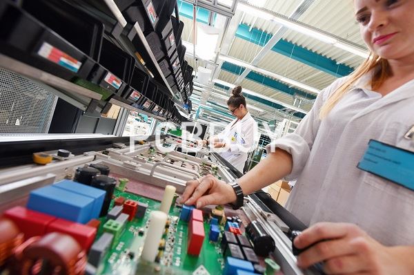
• Manual Soldering: Manual through-hole insertion is a straightforward process. Typically, one person at a single station will be tasked with inserting one component into a designated PTH. Once they're finished, the board is transferred to the next station, where another person is working on inserting a different component. The cycle continues for each PTH that needs to be outfitted. This can be a lengthy process, depending on how many PTH components need to be inserted during one cycle of PCBA. Most companies specifically try to avoid designing with PTH components for this very purpose, but PTH components are still common among PCB designs.
• Wave Soldering: Wave soldering is the automated version of manual soldering, but involves a very different process. Once the PTH component is put in place, the board is put on yet another conveyor belt. This time, the conveyor belt runs through a specialized oven where a wave of molten solder washes over the bottom of the board. This solders all of the pins on the bottom of the board at once. This kind of soldering is nearly impossible for double-sided PCBs, as soldering the entire PCB side would render any delicate electronic components useless.
After this soldering process is finished, the PCB can move on to the final inspection, or it can run through the previous steps if the PCB needs additional parts added or another side assembled.
Industry Category


