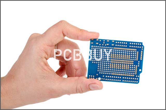
PCB stackup
By:PCBBUY 05/20/2021 17:30

PCB layering, or stackups, is simply a way to get multiple printed circuit boards in the same device by stacking them on top of each other while making sure there is a predefined mutual connection among them. These multilayer PCBs, which can multiply speed and functionality in a device, consists of at least three conductive layers, with the bottom layer synthesized with the insulation board.
While PCB stacking can confer a lot of advantages, including a reduction in impedance mismatch and signal cross-talk problems, there are also challenges that come with a printed circuit board layer stack.
In this passage, we will talking about all about PCB stackup, please check the content below for more details.
What is purpose of PCB stackups?
A PCB stackup refers to the arrangement of copper and insulating layers that make up a PCB. These layers are arranged in a way to get multiple printed circuit boards on the same device. At their most basic, multilayer PCBs consist of at least three conductive layers. The bottom layer is synthesized with the insulation board, and each circuit board layer is connected to the next.
While PCB layering creates a more complex and space-saving board, PCB stackups also offer the following advantages:
Maximize functionality: Multilayer PCBs can multiply the speed and functionality in the device, making for a more functional board.
Minimize vulnerability: Layer stacks can help protect internal layers from external noise, making it less vulnerable to damaging exterior forces.
Reduce radiation: Well-designed PCB layer stacks can help you minimize radiation from your device, especially in high-speed layouts. It is important to note, however, that poor designs with impedance mismatches can easily result in greater EMI radiation than a normal PCB.
Decrease costs: Good layer PCB stack-ups can also help achieve lower-cost manufacturing by placing multiple circuits onto a single board. One board means streamlined manufacturing for the board, the part the board will be used in and the packaging for the complete setup.
On top of these benefits, PCB stackups also reduce impedance mismatch and signal cross-talk problems. All these advantages make it highly desirable to make PCB stackups.

What are common types of PCB stackups?
Each type of board is described in more detail below, along with the conditions under which they are often used.
Each type of board is described in more detail below, along with the conditions under which they are often used.
2-Layer
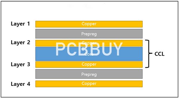
Often called double-sided PCBs, 2-layer PCBs are probably the most common types of multilayer PCBs as they can accommodate interconnects on both sides. These PCBs consist of three material layers, two of which are functional:
Signal layer: This top layer consists of copper with an approximate thickness of 0.0014 (1 oz.) inches to 0.0021 inches (2 oz.).
Laminate core: The laminate core separates the top and bottom copper layers, keeping them isolated. Vias create connections between the sides of the board.
Bottom layer: This second layer of copper is similar to the signal layer with an approximate thickness of 0.0014 inches (1 oz.) to 0.0021 inches (2 oz.).
These PCBs are inexpensive and relatively easy to produce, which is why they are often favored over the more expensive 4-, 6-, 8-, and 10-layer and up designs. They are also highly functional as there are no propagation delays, and they tend to have fewer potential design issues compared to other stackup options.
4-Layer
In terms of PCB stackups, 4-layer PCBs are the second most common option in multilayer boards. These PCBs have four layers to route electrical signals. These layers are sandwiched together, with a top and bottom layer on the outside and two inner layers contained between them. The top and bottom layers are where components and routing are placed. The inner layers, however, cannot make outside connections, so they are often used as power planes or for signal routing, which helps enhance the quality of trace signals and reduces EMI emissions. It is not recommended to make the inner layers signal layers — if you need four signal layers, it is recommended to look into a 6-layer board.
While more expensive to prototype and produce than 2-layer PCBs, 4-layer PCBs provide greater functionality overall. With thoughtful design, they can also provide excellent signal integrity and EMC capabilities.
6-Layer
A 6-layer PCB is functionally a 4-layer PCB with two additional signal layers. In total, 6-layer stackups include four routing layers — two internal and two outer — and two internal planes for grounding and power.
The design described above is the most common, as it balances high-speed signaling with EMI control. The design achieves this by running high-speed signals through the two buried layers while running low-speed signals through the surface layers.
However, this design isn’t effective for all applications. High-speed designs, for example, keep ground and power planes next to each other. Designs made for low EMI emissions, on the other hand, have extra ground planes to help with shielding. If you are wondering what design variation will best work for your application, always work closely with your online PCB designer and supplier to determine the best options.
8-Layer
The 8-layer PCB stackup offers even more options than the 6-layer board by adding two more layers for either routing or performance. It is also the first board listed that can achieve all five objectives for multilayer PCB design.
Typical 8-layer PCB stackups feature the power and ground layers in the center, offering good capacitance between layers as well as a separation between the second and third signal planes to protect signal integrity.
Industry Category


