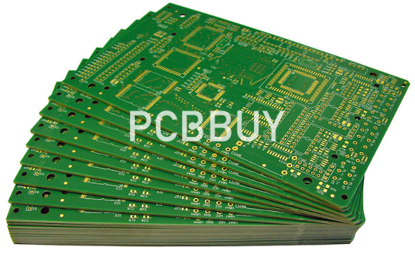
PCB substrate
By:PCBBUY 07/10/2021 17:25

The selection of PCB substrate will influence the performance, durability and quality of finished products. In this passage, we will lead you to learn everything about PCB substrate, how to select with different requirements. Come and check the content we prepare for you.
If you want to order PCB product, please check and custom your order online.
How surface roughness affects the quality of your PCB?
If your goal is to design a suitable circuit, you also need to consider how rough the copper foil surface will be. Roughing will ensure that the conductors have peel strength and that bonding of the substrate material and the copper foil is optimal. The standard roughness nowadays is set to around 5μm.
If you want to boost peel strength, it may be wise to embed hump on the foil into the substrate. In this case, you want to keep the roughness as low as possible (preferably up to 1.5μm, but no more than 3μm). You may be wondering how to peel strength will be kept if you reduce the foil roughness. The answer lies in the superior finish you apply to the surface of both the substrate and the foil. That way, the conductors can maintain optimal peel strength and ensure the reliable performance of your PCB.
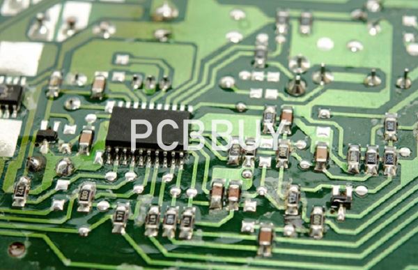
Copper foil requirements
PCB substrate materials play an integral role in determining the durability and quality of your board. It is noticeable that the manufacturers are trying to move towards fine lines and high density. You may have heard of the term HDI PCB. It stands for High-Density Interconnect Printed Circuit Board. Approximately ten years ago, a board needed to have line space (S) and line width (L) of not more than 0.1mm to be classified in the HDI category.
Today, the standards vary from one industry to another. Electronic products often have S and L set as low as 60μm, and they can even go to 40μm in advanced applications. During circuit pattern formation, S and L can reach a value as low as 30μm once you apply a thin substrate made of copper foil. The recommended thickness can go from 9μm to 12μm.
The problem is that CCL (copper clad laminate) that is so thin can be expensive and prone to defects. It is the best explanation for why companies resort to using 18μm-thick copper foil. However, if S and L are not more than 20μm, the copper foil of standard thickness might not be the best solution.
What types of substrate materials could be used in high-frequency PCBs?
You can find suitable material in one of the following:
• Fluorine-series resin – materials like PTFE have excellent dielectric performance and can be a great choice if you need at least 5GHz
frequency. Their cost is probably the highest of all three types, and they have a high thermal expansion coefficient. However, they perform impressively in areas of dielectric loss and constant and absorbing water.
• PPO or PPE resin – a suitable option for 1-10GHz frequencies. They secure an all-around decent performance of your board.
• Modified epoxy resin – they can also be the right choice for frequencies between 1GHz and 10GHz. In general, they have the most affordable cost, which is the reason for their popularity.
For example, we will consider PTFE, which falls into the fluorine-series category. It has excellent dielectric performance and can be a great choice if you need at least a 5GHz frequency. Please note that signal loss may also be due to the high roughness of the copper. It is why you should ensure to keep copper roughness under 1μm. Furthermore, it may be wise to go with roughness no bigger than 0.04μm.
We need to consider lamination material and its requirements if we are going to design HDI PCBs. Some considerations include dielectric performance, thermal capacity, insulation, and bonding. If you look at packages, the IC package may turn organic substrate from the ceramic. A decrease in the size of the FC package is noticeable as the values of S and L are around 15μm, with the tendency to become even more compact.
Multi-layered PCB substrate materials should reduce the thermal expansion coefficient and dielectric property while securing optimal resistance to heat. This type of substrate is the right choice as it can achieve all performance goals while maintaining an acceptable cost. We use SAP technology in the manufacturing process of circuits when their space and width are below 10μm. In fine circuit production on a large scale, MSPA can be applied to thin copper foil to insulate dielectric lamination.
How to choose PCB substrate materials?
You have the choice of picking from three different PCB types:
• Rigid
• Flexible
• Flex-rigid
The primary goal is to pick a board that will be perfect for your product. Many people aim for compact size and shape, but they forget about performance. Polyimide film can be a smart choice as it is versatile, and it can fit into different categories like black, white, and transparent. It also ensures a low thermal expansion coefficient while maintaining adequate resistance to heat.
Mylar substrate, on the other hand, is very elastic, and it has excellent resistance to environmental factors. On top of that, it is relatively affordable, which is why many users consider it. Flexible PCBs have to strive to achieve the same level of performance in terms of frequency and speed as standard PCBs. Advanced polyimide substrate and polytetrafluoroethylene are smart choices for flexible boards.
You can find flexible boards in many industries, including medicine, smart phone, and the gadget industry. That is why the market has been implementing changes in multi-layer boards that are flexible and extra thin (0.2-0.4mm). At this point, you can expect flexible boards to secure speed of up to 5Gbps, but you will need to use a low Dk/Df substrate material. It is also smart to use conductors that have over 100μm of thickness as that will help to handle the amounts of current and power.
Industry Category


