PCB tinning
By:PCBBUY 06/15/2021 17:56

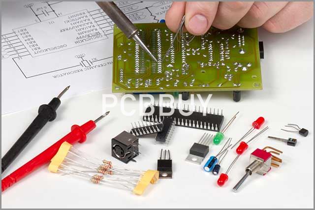
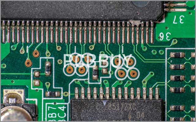
PCB tinning is to cover the untapped copper surface and create a solder mask with resins and paints. There is a better way to do this before copper oxidation and decomposition. It is called PCB tinning. PCB tinning is the process of coating copper traces with layers of tin, which will prevent it from any possible degradation, oxidation, or corrosion. The tin plating will also help mask copper traces while the circuit board itself is being etched.
In this passage we will focus on the PCB tinning, and please check the content we provide below for more professional knowledge.
What are the advantages of PCB tinning?
Doing this simplifies the manufacturing process and also prevents unwanted etching. The industrial method of manufacturing printed circuit boards uses strong solvents like sodium sulfate. Tinning will facilitate this since the risk of corrosion is much lower when a printed circuit board is tinned.
Also, the cost of placing copper traces with higher thickness levels on circuit boards with small current areas is much higher than usual. It is another reason why PCB tinning is preferable; it will save money, especially when there is a high existing path bridge.
What is the PCB tinning process?
How PCB tinning is performed?
As the name suggests, PBC tinning utilizes tin. The question is how this tin is used to mask the copper traces in a printed circuit board. The tinning process does indeed use pure tin. However, it also uses a soldered container, a mixture of lead and tin, mixed at a 60:40 ratio. Pure tin and soldered tin are what make up the base of the PCB tinning solution.
What is electroplating method of PCB tinning?
There are many ways to tin a printed circuit board physically, but the most common method is called the electroplating method. In this method, the circuit board is placed in a tin plating station. When this happens, the tin electrodes are introduced into the controlled current flow. It completes the first coating of soldered tin.
After the printed circuit board itself is entirely produced, the second coating of a tin can be applied. To create the second coating of tin, even more soldering must be done. The soldered layers of the container can be deposited either by hand or by a hot solder extruder, which will collect the soldered tin onto the area.
It will resemble liquid, which, if soldered correctly, will dry quickly as it is poured onto the copper trace. Like copper, the tin will also oxidize if exposed to outside environments. One of the reasons solder masking is applied is not to leave the circuit board unmasked.

Is PCB tinning necessary?
Recall that the entire purpose of PCB tinning is to prevent the copper materials in a printed circuit board from encountering corrosion if it is exposed to anything. Consider that any given printed circuit board will be exposed to some outside elements. PCB tinning will reduce the pressure from these external elements and impede the copper inside of the circuit board from oxidizing, if not halt it outright.
Some argue that PCB tinning is optional, and they would be correct. It is never a requirement for any given printed circuit board to be tinned. After all, it would operate the same without tinning as it would if it otherwise. The question, therefore, is one of longevity.
When a printed circuit board is tinned, it guarantees that the copper inside of the circuit board will last much longer. Additionally, PCB tinning will naturally enhance the current in the tracks of the circuit board and will allow it to operate and perform much more consistently.
A printed circuit board without any tinning can be compared to a house with an old and unstable roof. While the top will still protect from outside forces, it would not be nearly as effective as a brand new roof. PCB tinning will provide a "new roof" of sorts for the copper tracing inside of a circuit board.
What PCB tinning solutions are made of?
The Tinning solution is made up of many materials. Some of these materials are everyday items that can be bought locally, and some of these materials need to be purchased from merchants who specialize in PCB and PCB tinning materials.
While not all of these materials are necessary to make a tinning solution, select materials are indeed needed. Because so many variables go into a tinning solution, there are also many different ways to create PCB tinning from choose materials.
Thiourea - The essential ingredient for PCB tinning
The tin plating solution is made of the silver polishing agent, which is commonly used to clean jewelry. One thing that many do not know is that silver polish contains a compound called thiourea, which is the most necessary agent necessary for creating a tinning solution. Thiourea is combined with other materials to create a tinning solution. Without extracting the thiourea from silver polish, making a tinning solution from scratch is impossible.
Thiourea is so active on its own as a compound that it can create electroless tin plates with it that do not require a charge to conduct electricity. Since silver polish can be bought from a typical store, it is possible to at least create the base of any given tin plating with everyday items.
Other ingredients that will assist in creating a tinning solution
While thiourea is necessary to create a tinning solution, other materials will make creating a tinning solution a much easier process. The first of these is hydrochloric acid, which is also known as muriatic acid. Although this cannot be purchased directly as a silver polishing can, it can be made from household items.
Solid, lead-free solder is the second ingredient that can combine with silver polish to create a tinning solution. Soldering liquid is another thing that is not only essential to creating a tinning solution, but it is also crucial to designing printed circuit boards in and of them.
Industry Category


