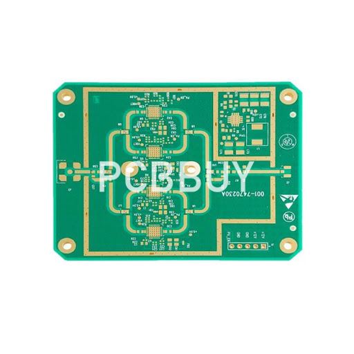
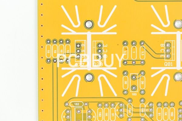
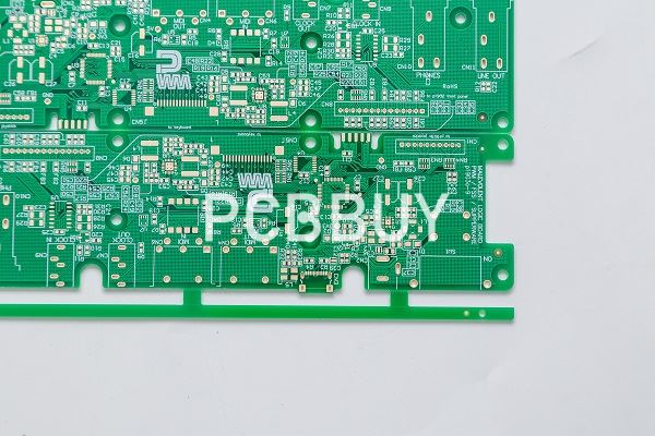
PCB trace impedance
By:PCBBUY 05/24/2021 18:39

In printed circuit boards, wires and traces are typically formed from copper because it is the least-resistant element apart from silver. Impedance, unlike resistance, is based on frequency. All wires and traces will generate at least some impedance to current flowing from any driver. Usually you may have a fairly fast rise time for your signals for trace impedance to become a problem.
Every trace has series inductance. It is distributed along the trace and is inversely related to the cross-sectional area of the trace. It is admittedly small, but it is non-zero. Therefore, for fast enough rise times, the impedance it offers can be significant.
And in this passage, we will focus on the topic - PCB trace impedance, and if you are going to know the performance of PCB product, please check the content below.
How Trace Impedance Works?
Every trace has a small, nearly indistinguishable series inductance distributed along the trace with an inverse relationship to the cross-section of the trace. As rise times increase, the resulting impedance becomes more noticeable. By the same token, each trace has capacitance distributed along the trace and the return path signal, which is a function of the width of the trace and the dielectric of the material between the signal return path and the trace. Once again, if rise times increase enough, the impedance generated as the current tries to flow through this capacitance can be significant.
Your drivers read all traces as distributed LC circuits and your trace AC impedance comes from this distributed LC circuit. This is considered uncontrolled impedance. We make no effort to design the trace environment to account for this impedance, allowing the inductance and capacitance to vary as it will along the trace. Since the resultant impedance usually has no effect on operations, there is no need to waste time or money designing ways to control it.
What Is Controlled Impedance?
But what if we are concerned about the effect of impedance on our operations? We can design a board where the trace looks like a transmission line, allowing us to avoid reflections by terminating it in its characteristic impedance. How does designing a controlled impedance circuit work?
When we control impedance, we make sure the impedance is constant at each point along the trace rather than varying from point-to-point as in a normal uncontrolled impedance situation. To control impedance, we need to control three features of the circuit’s geometry: the width of the trace, the spacing between the signal return path and the signal trace and the dielectric coefficient of the material surrounding the trace. You may also want to address the trace’s thickness. For example, a coaxial cable is a controlled impedance transmission line.
You can change these geometric features and still retain controlled impedance as long as you change other features as necessary so the relationship between these aspects does not change and impedance remains constant.
How Do We Determine Trace Impedance?
If we know the geometry of a trace and the properties of the material(s) surrounding it, how do we then calculate the trace’s impedance? In decades past we used various formulas for this. These formulas could be found in various application notes and industry standards, and they were “close enough” then to be suitable. But as requirements have become more precise, these older formulas are no longer considered reliable for the precision we now require. Our requirements became more difficult as we began to want formulas for edge-coupled differential traces, and there never have been reliable formulas for broadside-coupled differential traces.
What Is PCB Trace Impedance Formula?
To manufacture controlled impedance printed circuit boards, one must be able to measure impedance. The best way to calculate trace impedance is by using a trace impedance calculator. You can find trace impedance calculators online or in your CAD software. There are several parameters to consider when determining impedance, including:
Trace width
Trace thickness
Laminate thickness
Dielectric thickness
Copper weight
Once you have calculated all relevant parameters, you can adjust the all of the above (typically the trace width) to arrive at the impedance you are looking for. Once you think you are at an acceptable impedance, you can test the board’s effectiveness using test coupons manufactured on the same panel at the same time, so you can get a good impedance rating without the challenges of accessing the traces on the actual board. The test coupon traces should be identical to the board traces in order to get an accurate test.
Typically, the manufacturer will build test coupons on either end of the production panel so that by testing both coupons, you get a very reliable impedance reading without damaging the board. Testers measure impedance with a Time Domain Reflectometer (TDR) or a network analyzer.
Impedance can be measured using a network analyzer, a laboratory Time Domain Reflectometer (TDR) or a controlled impedance test system that employs TDR techniques. An engineer with practice using controlled impedance test systems will run the impedance test to ensure high-quality results.
Industry Category


