What is PDN in PCB and What Are the Functions of it?
By:PCBBUY 01/11/2022 11:04

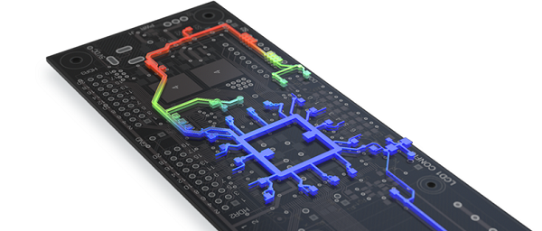
There are the power delivery network (PDN) challenges for a PCB designer, starting with the multiple instructions from hardware designer or power integrity (PI) engineer that are communicated by email, phone call, rules of thumb, etc. The designer must apply all of those instructions and rules to multiple power supplies.
In this passage, we will tell you everything about all the information about PDN in PCB. If you are curious about the PDN in PCB, please check and read the content below.

What Is PDN Impedance?
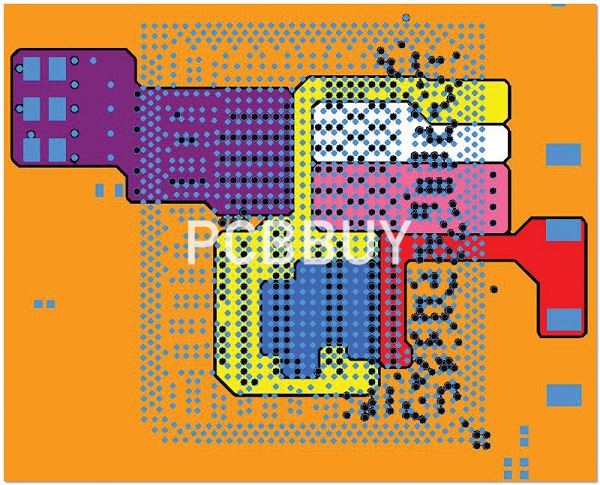
Every electronic system has a PDN, which stands for “power delivery network”. It’s basically every element that is connected to the voltage and ground rail, including the power and ground plane arrangement, any buses that connect from planes to groups of components, decoupling capacitors used for power stability, and any other copper features that connect or couple to the main power rails in the design. Parasitics also make up the PDN impedance, such as parasitic capacitance and inductance in any connections to ICs.
In particular, there are a few parasitic elements that are very important in determining the impedance of the PDN:
· Plane capacitance - the capacitance between plane layers in the PDN.
· Capacitor inductance - the leads on capacitors have some parasitic inductance, causing them to have a self-resonance.
· Trace inductance - traces that bring power to components also contribute some inductance to the PDN.
In addition to parasitic elements, capacitors are used on a DC PDN to help stabilize power by shunting high frequency noise currents to ground. Unfortunately, capacitors do not act like the theoretically perfect capacitors you find in textbooks, and they have the parasitic inductance mentioned above. These effects matter when we consider the transient response of the PDN to a pulse of current is drawn into the system by a load component on a power bus.
What is the target impedance of PDN in PCB?
The impedance of PDN is closely connected with the transient power supply current spectrum of digital IC. In some designs, there are as many as 10 kinds of power supply voltages. The power supply voltage, power ripple index, working condition and transient power current spectrum of different IC may be different. Therefore, the target impedance of PDN (and the maximum allowable impedance of PDN) of different IC is different.
The design objective of PDN is that the impedance of PDN is lower than the target impedance within the current spectrum of the transient power supply. For example, on one hand, if it is higher than the target impedance, it would result in excessive ripple index of the power supply, on the other hand, if it is significantly lower than the target impedance, it would also unnecessarily increase the design cost. Therefore, it is important and complex to determine the target impedance of PDN.

How to lower the PDN in PCB?
The idea behind FDTIM is to ensure that the PDN design meets the target impedance and the values for the relevant frequency range stay below the given limits. Yet this is easier said than done. A PCB usually contains dozens of active components, often several hundred capacitors and inductors with all their parasitic characteristics (e.g., ESL and ESR of the capacitors). There are also other parasitic inductors on the different PDN elements (e.g., pads/land patterns, vias, and traces) that can heavily affect PDN impedance values.
To lower the impedance of the PDN, engineers can tweak two general things: Reducing the inductance and/or increasing the capacitance of the PDN. The placement and the value of decoupling capacitors play an important role in such an optimization, as this will affect both, the capacitance and the inductance of the PDN. Placing the capacitors on the same layer as the IC supply pins for example would minimize the inductance. Unfortunately, this is often not possible for space or manufacturing reasons. Nevertheless, if resonance peaks are revealed in a PI analysis, the copper shapes of the PDN most likely have to be modified to eliminate these peaks efficiently.
What is transient response in PDN design?
Note that even if the impedance band is flat between the clock and knee frequencies, the transient response can still appear as an underdamped oscillation. It is best that you also use one or more decoupling capacitors on your PDN to change the damping level for any transient oscillation in the PDN. The goal is to bring the transient response into the overdamped regime. Take a look at our simulation guide to learn more about these techniques.

The best way to do this is to determine the appropriate decoupling capacitance that will compensate for the transient response and transition the response to critical damping. Learn more about sizing decoupling capacitors and working with plane inductance in my recent articles on Altium’s PCB design blog. Note that, when you include a decoupling capacitor in your schematic, you should account for the capacitors’ self-resonance frequency.
Even if you size your capacitor to provide the required charge to compensate the transient current, you may still see some ringing on the power rails as you are still not in the critically damped or overdamped regime. In this case, you can simply use a larger capacitor. Normally, it is better to use multiple decoupling capacitors in parallel on the PDN rather than a single larger capacitor as this ensures the self-resonance frequency of this decoupling capacitor group will be larger than that for a single capacitor.
Industry Category


