PDN in PCB
By:PCBBUY 09/07/2021 09:09
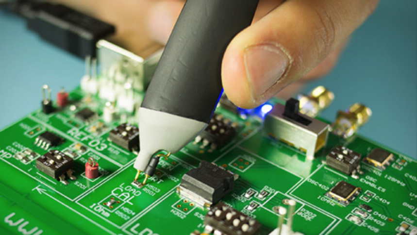
Do you know the importance of designing a good power delivery network (PDN) into our PCB?
They are no less damaging as an incorrectly designed PDN can cause intermittent problems to outright failures of the circuit board.
If you are curious about it, please check and read the content we prepare below. Let’s dive into the importance of how we design the power delivery network of our circuit board with this—your PDN design guide.
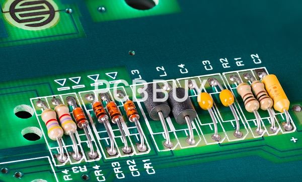
Why PDN is important to PCB?
In PCB design, DC analysis is vital as numerous factors combine to exacerbate the problem of power integrity. Core voltage levels continue to drop; 1.2V and less are now common. As voltage is reduced, current requirements typically increase (IR drop = I * R). The miniaturization of electronics results in fewer layers and higher densities, thus reducing the available area for power nets. And antipads around vias perforate the planes and can overlap, creating the “Swiss cheese” effect.
In addition, there are the power delivery network (PDN) challenges for a PCB designer, starting with the multiple instructions from hardware designer or power integrity (PI) engineer that are communicated by email, phone call, rules of thumb, etc. The designer must apply all of those instructions and rules to multiple power supplies. Having done that, the designer must then attempt to fulfill additional requests, such as “Can you shrink it by 20%?”, “Can you remove two plane layers and five capacitors?”, and that age-old favorite, “Can you do it yesterday?”
Electromagnetic interference (EMI)
The faster the circuitry became, the more sensitive it could be to EMI from both internal and external sources. One way to guard against EMI problems is to configure the power and ground planes to shield against both incoming and outgoing interference.
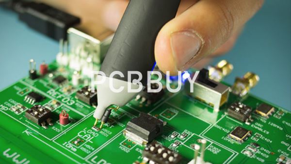
Ground bounce
When a lot of digital signals are switching states at the same time, it can produce an effect known as simultaneous switching noise (SSN) or ground bounce. This can be seen in memory or data buses, and if the rapid switching causes the signals to not return to their reference ground level, they will bounce above it. This effect can produce undesirable noise in the circuits that could potentially create false switching and disrupt the operation of the device. A well designed PDN can help control the reference ground level.
Power ripples
Switching may also be caused by a power supply, which will create noise, or ripples, in the circuitry. These ripples can manifest themselves as crosstalk in other circuitry, which can adversely affect the signals in those circuits.
What is PDN impedance in PCB?
Every electronic system has a PDN, which stands for “power delivery network”. It’s basically every element that is connected to the voltage and ground rail, including the power and ground plane arrangement, any buses that connect from planes to groups of components, decoupling capacitors used for power stability, and any other copper features that connect or couple to the main power rails in the design. Parasitics also make up the PDN impedance, such as parasitic capacitance and inductance in any connections to ICs.
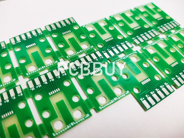
In particular, there are a few parasitic elements that are very important in determining the impedance of the PDN:
· Plane capacitance - the capacitance between plane layers in the PDN.
· Capacitor inductance - the leads on capacitors have some parasitic inductance, causing them to have a self-resonance.
· Trace inductance - traces that bring power to components also contribute some inductance to the PDN.
What is the importance of PDN impedance in PCB?
The high speed and high frequency designers reading this will already know the answer to this question. However, with technological demands mounting, we’ll all be high speed and high frequency designers sooner than we like, so it is important to understand how PDN impedance affects the behavior of signals in your PCB. Unfortunately, we don’t always do the best job of placing this information in one place, so I’ll happily do this here.
In short, your PDN impedance will affect the following aspects of your circuits:
Power bus noise
The voltage ripple created due to transient currents in your PCB. Note that, because your PDN impedance is a function of frequency, the voltage ripple caused by a switching will also be a function of frequency. Note that these transients can arise regardless of the level of noise in the output from your voltage regulator.
Damping in power bus noise
Any ripple on the power bus could appear as ringing (i.e., an underdamped transient oscillation) in some cases. This is one problem that can occur if your decoupling capacitor is incorrectly sized or if you do not account for your decoupling capacitor’s self-resonance frequency in your decoupling network.
Required level of decoupling
Most capacitors have become insufficient for ensuring decoupling in PCBs with fast logic due to their relatively low self-resonance frequencies (~100 MHz). Therefore, designers used interplane capacitance to provide sufficient capacitance to ensure decoupling. Newer capacitors with GHz self-resonance frequencies are also available, and the combination of these is used to provide decoupling in high speed/high frequency PCBs.
Industry Category


