What is PTH in PCB based in 4 Main Aspects for beginners?
By:PCBBUY 11/15/2021 10:08

Plated through holes must meet some conditions to be processed as plated holes, otherwise, they will be considered as non-plated ones. Sometimes, PCB designers expect certain features in the manufactured PCBs, but receive something different in the end. Mounting holes and slots are examples of that.
Are you a beginner of PCB world? If you are going to learn the details about c, please check and read the content below in this passage.
1. What is the basic information of PTH in PCB?
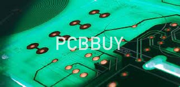
Printed Circuit Boards electrically connect electronic components through conductive pathways, tracks or signal traces that are etched onto a copper-plated sheet. The PCB board itself is made of a non-conductive substrate and has several holes drilled through it. These holes are drilled with coated, solid, tungsten carbide drill bits and are prominent in diameter. The holes are made conductive by electroplating with copper.
By using PCBs “through-hole” or “thru-holes” technology, electronic components are mounted onto the substrate using the components’ legs (or leads). The leads are placed into the holes and soldered onto pads on the opposite side through manual assembly (placing by hand) or using automated insertion mount machines.
Printed circuit boards may have different sized holes, which are differentiated as PTH (Plating-Through-Hole), which has been described above, and NPTH (Non-Plating-Through-Hole), which have no coating as they are not used for conducting pathways.
2. How to process PTH in PCB?
TH or Plated-Through-Hole PCBs are ones in which the leads (or legs) of electronics components are inserted into designated ‘holes’ in the printed circuit board. These are soldered into place using a number of soldering techniques such as using a hand solder, selective soldering, wave solder, or intrusive reflow process. This entire process is called conventional assembly. Soldering forms very strong joints as the component are soldered completely through the PCB and not just onto the surface of the PCB like Surface Mount Technology (SMT) components.
The components inserted in a PTH PCB are done through these automated processes:
· Radial insertion (electrolytic capacitors),
· Axial insertion (resistors and diodes),
· Odd form insertion (connectors, transformers, etc.) or
· Manually (by hand.)
3. What is the work principle of PTH in PCB?
PTH plays a role in depositing a thinner electroless copper with chemical process to be the later substrate of copper plating on a drilled and non-conductive base material of hole wall.

How to decompose for PTH?
PTH decomposable process: alkaline cleaning→class2 countercurrent rinsing→roughening(mircoetching)→class2 countercurrent rising→pre-dip→activating→class2 countercurrent rising→desmearing→class2 countercurrent rinsing→PTH→class2 countercurrent rinsing→picking
4. How to control the cost of PTH in PCB?
For standard PCBs, how to design the holes, annular rings and hole density will have effect on your PCB cost. Here are some ideas for reducing your cost.
Larger Holes: When it is feasible, use larger diameter holes and annular rings. To manufacture small holes, high precision machines are required; these machines always cost more to use so PCB fabricator often adds an upcharge for holes in diameter between 0.15mm and 0.3mm. To determine the added cost, you will need to contact the MADPCB to learn our policies about additional charges for hole sizes of standard printed circuit boards.
Larger Annular Rings: Minimum annular ring is a vital requirement that refers to through hole pads and vias only, and it is defined as the border of the hole’s and the pad’s minimum distance. That is, it is the copper rings smallest width the limits the hole. It is important to know that the cost of the PCB will be higher if the minimum annular ring is less than our standard requirements. A round through hole pad or via annular ring width is homogeneous around the hole, while the width of an oblong-shaped through hole is non-homogeneous. No matter round-, or oblong-shaped through holes, just keep in mind, using larger annular rings will decrease the PCB cost since high efficiency, and increase the PCB quality since no need to worry drilling tolerance or shaving rings.
Lower Hole Density Per Square Meter: No matter mechanical drilling or laser drilling, the machines have their own efficiency. High hole density per square meter, especially for PCB mass production runs, it will spend longer time to finish the drilling process, PCB fabrication house will charge additional drilling cost. If it is possible in your PCB design, decreasing the hole density per square meter will cost your less in cost.
Industry Category


