What is Populated PCB & What is the Process of It?
By:PCBBUY 01/17/2022 09:49

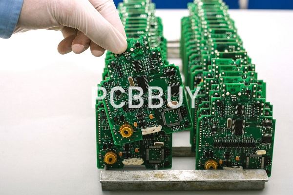
A populated PCB is a circuit board with electronic components. A board without electronic components mounted on it is a bare board. This means a PCB can either be bare or populated. PCBs can be populated through surface mount technology or through hole technology.
Are you going to learn the knowledge of populated PCB? If you are going to search the information of populated PCB, please check and read the content below for more in this passage.
What is the basic definition of populated PCB?
Manufacturers solder the electronic components on the PCB to achieve a populated PCB. The populated circuit board comprises components such as IC, capacitors, and diodes. While a populated PCB features electronic components, a bare board doesn’t.
It is important to understand that a populated PCB is different from PCB manufacturing. The process of PCB manufacturing entails the production of a bare board. The manufacturing process involves creating a PCB prototype. The method of populating a PCB depends on the purpose of the circuit board.
PCB population involves several processes. It is important manufacturers carry out each of these processes carefully. To carry out PCB population, you will need the following;
· Bare PCB
· Soldering materials
· Soldering flux
· Electronic components
· Soldering equipment
Each of these equipment is very important during PCB population. The bare board serves as the foundation of the populated PCB. It is a core material in PCB population. Manufacturers either use SMT or THT to mount components on a bare board.

What is the process of PCB population?
Checking for these errors and misalignments can involve one of several different inspection methods. The most common inspection methods include:
Manual Checks
Despite upcoming development trend of automated and smart manufacturing, manual checks are still relied on in PCB assembly process. For smaller batches, an in-person visual inspection by a designer is an effective method to ensure the quality of a PCB after the reflow process. However, this method becomes increasingly impractical and inaccurate as the number of inspected boards increases. Looking at such small components for more than an hour can lead to optical fatigue, resulting in less accurate inspections.
Automatic Optical Inspection
Automatic optical inspection is a more appropriate inspection method for larger batches of PCBAs. An automatic optical inspection machine, also known as an AOI machine, uses a series of high-powered cameras to "see" PCBs. These cameras are arranged at different angles to view solder connections. Different quality solder connections reflect light in different ways, allowing the AOI to recognize a lower-quality solder. The AOI does this at a very high speed, allowing it to process a high quantity of PCBs in a relatively short time.
X-ray Inspection
Yet another method of inspection involves x-rays. This is a less common inspection method — it's used most often for more complex or layered PCBs. The X-ray allows a viewer to see through layers and visualize lower layers to identify any potentially hidden problems.

What are the techniques of PCB population?
Manufacturers carry out PCB population using two major techniques. These techniques are surface mount technology and through hole technology. SMT and THT are common ways to populate a printed circuit board.
SMT
This is a common way of populating a circuit board. Manufacturers use SMT for mounting sensitive components. In Surface mount technology, the components feature short leads. Furthermore, this technique uses automated machines to populate components on circuit boards. SMT involves mounting SMD s directly on the PCB. Manufacturers populate this circuit board with the use of pick and place machine.
THT
The through hole technology involves inserting the pins of the components into the holes of the board. Here, the placement of components must conform to the standards of the THT process. Manufacturers make use of tweezers to place a component on the circuit board in this technique.
However, in THT, manufacturers place components with leads via plated through holes. This was a common technique for populating boards before the advent of SMT.
Industry Category


