Prepreg and core in PCB
By:PCBBUY 06/28/2021 17:08

Prepreg is a dielectric material that designers pack in between a copper and a Core or between two Cores in a PCB to provide the required insulation. Prepreg is simply an insulation layer. Since it can bind a copper foil and a Core, it is safe to refer to it as a binding material. Users can also modify Prepreg to their needs as peculiar dielectric materials. They can also use a chemical process to transform a certain part of a Prepreg into a conductive region through the combination of specific catalysts and additives.
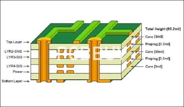
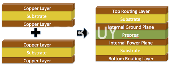
The PCB Core is the glass-reinforced epoxy laminate sheets and copper traces’ FR4 layers. The Prepreg binds the layers and PCB Core together when users heat the Core. In this passage, we are talking about the roles of Prepreg and core in PCB. Come and check the content we provide below for more detailed information.
What are the differences of Prepreg and core?
PCB cores and laminates are similar and quite different. Your core is effectively one or more Prepreg laminates that are pressed, hardened, and cured with heat, and the core is plated with copper foil on each side. The Prepreg material is impregnated with a resin, where the resin is hardened but left uncured. Most manufacturers describe the prepreg as the glue that holds core materials together; when two cores are stacked on each side of a prepreg laminate, exposing the stack to heat causes the resin to begin bonding to the adjacent layers. The hardened resin slowly cures through cross linking, and its resulting material properties start to approach those of the core layers.
The resin material encases a glass weave, and the manufacturing process for this glass weave is very similar to that used to manufacture yarns. The glass weave can be quite tight (e.g., 7628 prepreg) or loose (e.g., 1080 prepreg), which is controlled with a loom during manufacturing. Any gaps and the overall homogeneity of the yarn will determine the electromagnetic properties, which is then responsible for dispersion, losses, and any fiber weave effects seen by signals in the board.
PCB core vs. prepreg materials can have somewhat different dielectric constants, depending on the resin content, type of resin, and glass weave. This can be a problem when designing boards that require very precise impedance matching as the effective dielectric constant seen by a signal on a track depends on the dielectric constants of the surrounding materials. Not all prepreg and core materials are compatible with each other, and core/prepreg stacks with very different dielectric constants make it difficult to predict exact dielectric constants and losses in an interconnect .
With any PCB core or prepreg material, creepage and leakage current is a concern at high voltage. Electromigration of copper and subsequent growth of conductive filaments are one reason for creepage specifications for FR4 materials. This problem, as well as a desire to increase glass transition and decomposition temperatures, motivated a switch to non-dicyandiamide (non-DICY) resins in FR4 cores and laminates. Phenolic resins provide higher decomposition and glass transition temperatures compared to DICY resins while also providing higher insulation resistance after full curing.
What are the applications of Prepreg and core?
Multi-layered boards
What holds the layers together is the multi-layered board of Prepreg. The user will need to fuse them when they stack all the board’s layers by exposing it to high temperatures. They will then have the similarity between the overall board thicknesses with the Prepreg thickness. When the designers use the Prepreg on a multi-layered board, it must have specific characteristics. The new surface must not have excessive resin powder, cracks, foreign matter, defects, stains, or oil. It must have a smooth feel and look.

Complex PCBs
Engineers will probably have a more complex Prepreg if they have a complex PCB. As a result, they can only achieve the needed thickness for the board and Prepreg to use different types of Prepreg.
What is the effective dielectric constant of Prepreg and core?
With the obvious structural variations in core and prepreg materials, getting an accurate value for the dielectric constant and loss tangent is important from a signal integrity standpoint. When your signals have low rise time, you can probably get away with taking a value from a marketing datasheet. Once your knee frequencies or analog signals hit the GHz range, you need to be careful with values quoted from datasheets, especially when modeling interconnect behavior and using impedance controlled routing.
The problem with datasheet values is that the actual dielectric constant measured depends on the test method, routing geometry, specific frequencies (especially in the GHz range), resin content, and even material thickness. The weave pattern in PCB core/prepreg materials makes them highly inhomogeneous and anisotropic, meaning the important material properties vary in space and along different directions. This is the reason we have fiber weave effects, such as skew and fiber cavity resonances.
You might be thinking, why should the thickness of a laminate matter when characterizing material properties? The reason is that the important parameter that characterizes signal behavior is the effective dielectric constant (remember, this is a complex quantity!), which depends on the trace dimensions and layer thickness you use in you material. Take a look at these articles for microstrip and symmetric stripline transmission lines.
Finally, the other important parameter to consider is the copper roughness on a given laminate. The two articles I linked to above provide effective dielectric constant values for microstrip and stripline transmission line geometries while assuming no copper roughness. However, there is a simple linear approximation you can use to account for copper roughness:
If you’re working at extreme high speeds/high frequencies with low signal levels, and you require highly accurate interconnect characterization, then your best bet is to create a test coupon and use a standard measurement to determine the effective dielectric constant. Your test method should use a geometry that closely matches your intended interconnect geometry. This takes some work on the front end, but accurate test and measurement could save you unnecessary prototyping runs on the back end.
Industry Category


