QFN package
By:PCBBUY 08/14/2021 09:37

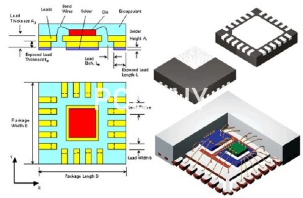
QFN stands for quad flat no-lead package. It is a leadless package that comes in small size and offers moderate heat dissipation in PCBs. Like any other IC package, the function of a QFN package is to connect the silicon die of the IC to the circuit board.
In this passage, we will talk about the detailed knowledge of QFN package of PCB. Please check and read the content below we prepare for more information.
What is the structure of QFN package in PCB?
The QFN packages come with a die that is surrounded by a lead frame. The lead frame is made up of a copper alloy with a matt tin coating.
The die and the frame are usually connected to each other using wire bonding. Copper/gold is usually preferred for wire bonding. Some manufacturers use flip-chip technology for this interconnection. The flip-chip technique offers better electrical performance compared to the conventional one.
The metalized terminal pads are located at the bottom surface. These terminal pads are present along the four edges of the bottom surface and provide electrical interconnections to the PCB.
The bottom side of the package consists of an exposed pad. This pad provides an efficient heat path to the PCB. The exposed pad enables ground connection as well. The QFN package is soldered to the circuit board at the exposed pad. The die attach is the epoxy material used to fix the die to the exposed pad.
For thermal management in PCBs, check out 12 PCB Thermal Management Techniques to Reduce PCB Heating.
The following are some of the properties of standard QFN packages:
· 0.35mm to 2.10mm maximum seated height (standard: 0.85 mm)
· Terminal plating of Ni-Pd-Au and Sn
· Halogen-free and lead-free
· RoHS, ELV, and REACH compliance
What are the advantages of QFN package?
·Quad flat no-lead packages come in lightweight and are easy to handle.
·These packages are available in a thin profile and a small form factor.
·The bond wires that are used to connect the die and frame are short.
·The lead inductance of these packages is low.
·They are ideal for applications that require good heat dissipation.
·These packages are easily available at a low cost.

What are the main types of QFN package?
Based on the method of molding, the QFN packages are classified into punch-type and sawn-type packages.
Punch-type
In punch-type singulation, the package is molded in the single mold cavity format and is separated using a punch tool. This means that only a single package is molded into shape using this method.
Sawn-type
These packages are molded using the mold array process (MAP). This method involves cutting a large set of packages into parts. A final saw process helps to separate the sawn-type packages into individual packages.
How to solder QFN on PCB?
Soldering is a part of the QFN assembly process. During the assembly process, the components are mounted after solder paste screening. After QFN components are mounted using a pick and place tool, they are soldered using reflow soldering. When the PCB board goes into a reflow oven, the temperature inside will make certain areas of the board heat faster than the rest. The heavier components and large copper areas will take more time to get heated.
The top surface temperature of the QFN package is monitored using thermocouples throughout the process. This is to check that the peak package body temperature (TP) does not exceed the standard values.

How are the QFN solder joints inspected?
The solder joints of the QFN components are formed underneath the package. Hence for the inspection of these, optical inspection and X-ray inspection are used.
Rework on assembled components
If a defect is noticed post assembly on any QFN component, that particular component can be removed and replaced. Special rework stations are available for this purpose. A rework station should have the following components.
· Split-light system: acts as a vision system to observe the bottom side of the package and the site on the PCB.
· An X-Y table for alignment.
· A hot-air system with top and bottom heaters for component removal.
The procedure for rework is given below.
· A pre-bake process is done before heating to avoid any moisture-related failures of the board and the components.
· The next step is de-soldering and the temperature profile of the board and the components should be kept in mind.
· Once de-soldering is done, the component should be mechanically removed. For large components, pipettes can be used and for smaller ones, tweezers are a good option.
· After removal, the PCB pads should be cleaned to remove any solder residue. This also prepares the site for the new component placement.
· The placement of the new component takes place through the same steps mentioned earlier during assembly.
Industry Category


