What is RF PCB Design with 7 Primary Elements for Designers?
By:PCBBUY 11/26/2021 10:27

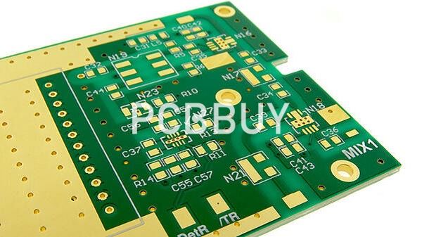
It is a significant difference between RF PCBs and standard PCBs. The issues that surround RF PCB design will come back to this, as micromanaging high frequencies are integral to designing an RF PCB. Choosing the right materials is the most crucial aspect when it comes to RF PCB design. Whether you want to use two layers or four layers, materials will make or break an RF PCB. There are three things to consider when choosing RF PCB materials.
If you are searching for the basic information of RF PCB design, please check and read the content below in this passage for professional knowledge.
1. What is the introduction of RF PCB design?
RF circuits are non as intuitive as typical circuit diagrams, and sometimes a diagram may appear to violate basic electrical design rules. However, due to the propagating nature of the electromagnetic field, circuits running at RF frequencies act very differently from typical integrated circuits operating at DC or in digital bands. Whether you’re designing a system for wireless communication or just need to design a transmission line with specific impedance, pay attention to these basics of microwave engineering.
2. How to choose material for RF PCB design?
FR4 materials are acceptable for RF transmission lines and interconnect operating up to WiFi frequencies (~6 GHz). Beyond these frequencies, RF engineers recommend using alternative materials to support RF signal propagation and printed RF circuit designs. Standard FR4 laminates use resin-filled fiberglass weaves to hold components, but these fiber weave effects in certain materials could create signal and power integrity problems if fabrication procedures are not specified properly.
Alternative material systems use PTFE-based laminates and bondply materials to bond a PTFE layer with the next layer in your PCB stackup. These materials have lower loss tangent than FR4 materials, so signals can travel farther without attenuating and still fall within acceptable margins. These laminates should form the substrate that supports RF transmission lines at very high frequencies, such as 77 GHz radar, or for very long interconnects at lower frequencies, such as 6 GHz WiFi. The table below summarizes some important material properties for common RF PCB materials.
3. What is RF reflection in PCB design?
RF reflection functions similarly to how sound is bounced back and creates an echo. It’s also analogous to waves of water crashing and bouncing back. The reflection occurs because the wave encounters a discontinuity of the medium that it’s traveling, and that’s the same for reflected RF waves.

RF reflection must be considered when discussing transmission lines. One of the basic principles of transmission lines is to ensure that the characteristic impedance of the driver, traces, and load are matched. Characteristic impedance is not defined by the resistance or the trace length but rather determined by the dielectric, trace width, and the separation between the trace and the plane.
4. How to process RF PCB design?
RF PCBs are one of the fastest growing sectors in PCB manufacturing. With with proliferation of IoT sensors, wireless electronics, and smart phones, it’s easy to see why. But how do you know if you’re working on an RF PCB? The PCB industry considers any board that operates above 100MHz to be an RF PCB. Anything about 2GHz is a Microwave PCB.
Using Vias for Transmission Line Layer Changes
Does your RF layout require you to move a transmission line between layers? Maxim recommends using at least two via holes for each transition point to minimize via inductance loading. The width of these transition vias will need to match the width of the transmission lines. Used effectively, these vias can help to cut transition inductance by 50%.
5. What are the applications of RF PCB design?
RF boards have a multitude of different applications, including wireless technologies, smart phones, sensors, robotics and security. With the advent of new technologies that are pushing the limits of electronics, the demand for RF boards is on the rise.
Finding a capable RF PCB manufacturer is critical to make sure the boards are fabricated to high quality standards and on-time. Our reputation speaks for itself. We pride ourselves on bringing the most demanding layout concepts to reality.

6. How to place the components of RF PCB design?
When placing components on an RF circuit board, the needs of the circuitry often demand a tighter part placement. Modifying the component placement is one of those compromises that the designer must carefully manage to ensure that the board can still be built with standard automated assembly equipment to keep production costs from escalating. RF boards also tend to have more metal on the external layers for their power networks, and components are often placed directly on those areas. While this connection may be better for the performance of the RF circuitry, it can cause problems for PCB assembly.
7. How to build RF PCB?
The CM will also need to be provided with some additional information before building the board:
· Is the board a new design or a modification of an existing one? New boards will require additional review to ensure that nothing is missed while existing designs will typically have already gone through those steps.
· How much experience does the design team have with the target application of the board design, and how much general RF experience do they have? The answer here will give the PCB CM an understanding of what to look for during their reviews.
Industry Category


