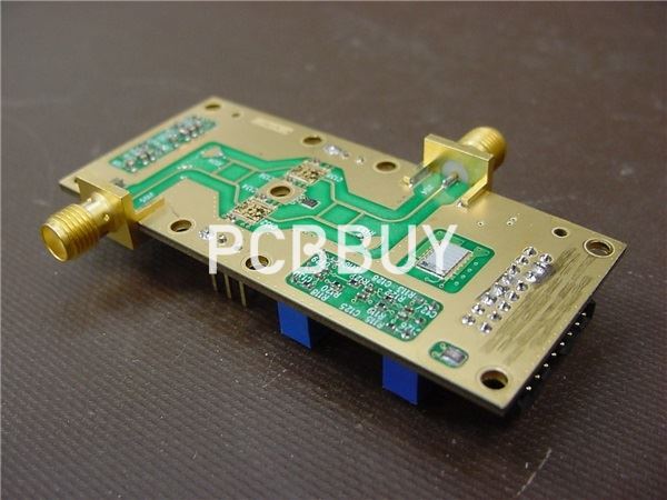
RF PCB design
By:PCBBUY 07/07/2021 17:21

RF stands for "radio frequency." It makes the PCBs a part of operating at a much higher frequency than standard PCBs, starting from 100 megahertz (MHz).
It is a significant difference between RF PCBs and standard PCBs. The issues that surround RF PCB design will come back to this, as micromanaging high frequencies are integral to designing an RF PCB.
In this passage, we will focus on the RF PCB design and tell you everything about it. If you are going to learn the professional knowledge, Come and check the content we prepare for you below.
What are the basic types of RF PCB design?
The higher frequency of RF PCBs makes it more complicated in their creation and design. There are four factors to consider before developing a blueprint for designing an RF PCB.
Some Constants
The first difference between RF and non-RF PCBs are the constants. Dielectric constants, for example, can be treated as a single value in non-RF applications. But because the frequency of an RF board is much higher, they should be treated as multiple values.
Temperature control
Due to the higher frequency used in RF PCB, temperatures within the board can fluctuate. If the materials used to create the board are not appropriately placed, these fluctuations can get out of hand.
Adjacent spacing
The most optimized RF PCBs contain four layers. Constructing a four-layer PCB means that individual components will need to be spaced together in a way where everything can work together correctly.
Material selection
It is creating a four-layer PCB that has consistent temperatures demands that you choose materials that will allow the least margin for error. Read to discover exactly what these materials are and how to use them.
How to choose material for RF PCB?
Choosing the right materials is the most crucial aspect when it comes to RF PCB design. Whether you want to use two layers or four layers, materials will make or break an RF PCB. There are three things to consider when choosing RF PCB materials.

The coefficient of thermal expansion
This coefficient pertains to an object's size about temperature changes. Because RF PCBs deal with temperatures that are not only high but variable, this coefficient requires continuous use as a method of micromanaging temperature levels.
Moisture absorption
Moisture must also be taken into account as water affects temperatures since moisture does affect temperatures. Moisture is directly related to the environment that the device utilizing the RF PCB operates in.
Cost vs. Performance
If this debate wasn't relevant enough when selecting non-RF PCBs, it is even more relevant when selecting materials for RF PCBs. The best thing to do is to know what your budget is to the penny, then aim to choose a cost-balanced material, electrical performance, and thermal robustness.
What are the instructions of RF PCB design?
Because so many things are at work when it comes to RF PCBs, the design layout will affect the stability and reliability of the final product.
Everything in an RF PCB needs to come together, so there is not a lot of crowding, yet nothing is too far apart. These instructions will show you how to do this.
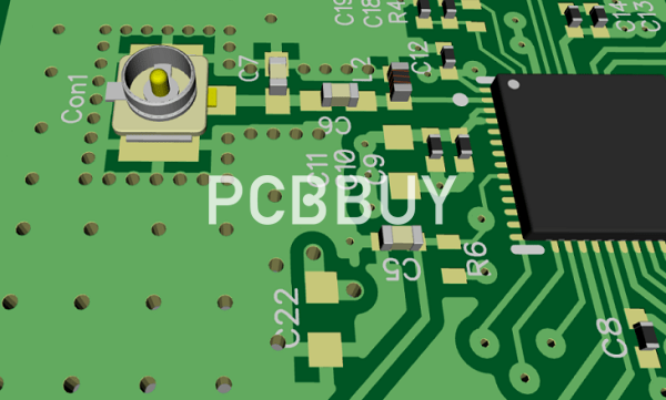
Arrange RF traces first
RF traces carry the highest frequency of an RF board. These are arranged first because everything else will be placed around them.
Another thing that must be done is to leave adequate space. It will allow smoother bends, and more importantly, it will isolate the RF signal.
Isolating RF tracking is essential.
After you have arranged the RF traces, you must now design your board such that the RF tracks are isolated. You can do this by stitching vias around the RF traces.
It is essential because it is very likely that the RF board you are designing will be part of a device that utilizes high-speed signals, such as USB and HDMI ports. Isolating the tracks will prevent overheating when these signals are sent to and from the device.
Keep battery inductance low
Ground inductance is affected by two things in the RF chipset: Vias and through holes. Vias can accomplish the task of connecting ground pins to the ground plane.
Arranging multiple through holes will also reduce the harmful effects of the ground plane, and this is important because battery inductance does not respond well to high frequencies.
Industry Category


