SMD in PCB
By:PCBBUY 06/05/2021 17:55

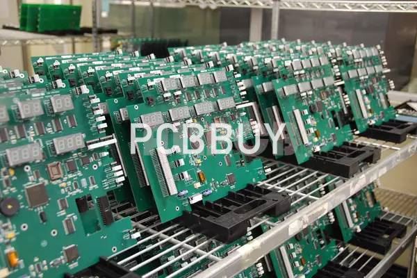
In simplest terms, a surface mount device (SMD) is an electronic device that you would use on your projects. Every electronics engineer eventually needs to use them. These devices are typically found on a printed circuit board.
Day by day, electronic components are getting smaller in the printed circuit board market. It would help if you also evolved your projects with the need to ensure your survival in it.
The new components revolving in the market are not only small but are also cheap and fast. They go by the name of surface mount devices (SMDs). Have you ever heard of them? This article will cover everything that you need to learn about them. Let's get started and read the content below.
What are the advantages of SMD products?
Dependable Processing
Some manufacturers are using high-performance plastic LCP for making surface mount devices. It makes sure precise grid alignment and maximum dimensional stability. The material has tremendous solder heat resistance. Therefore, a smooth, dependable SMD connection system is guaranteed.
You will not need to pre-dry such SMDs as they have low moisture sensitivity (MSL 1). They also have a low thermal expansion coefficient, which prevents a PCB assembly from being dismantled during soldering. Therefore, you can rapidly perform the whole automatic PCB assembly process.
Stable Solder Connections
The PCB terminals of SMDs made using LSF make sure a firm grip on the board. It is because the manufacturers use two solder pads for each pole. You can even place large electronic components as the holding force/pin is more than 150 N.
Manufacturers also perform endurance tests to make sure the shock resistance and high vibration are according to IEC 61373/10.2011. Thus, you will get a maintenance-free and smooth SMD process in the long run.
Not just this, you will also get good results with composite PCBs made of aluminum, ceramics, or glass.
Effective Assembly
SMD with suction surfaces support and pick-and-place pads ensure accurate placement and safe mounting in the automatic PCB assembly process. You will also be maximizing the performance of the assembly due to the lightweight of the PCB terminals of SMD.
Coming to the packaging of these components, you will get them in standard conveyor widths with tape-on-reel packing. Furthermore, they are made for automatic processes and thus contain many numbers of features for every roll. What does it mean? It just means that you are reducing your setup expenses.
So, you already know the benefits of surface mount devices. In the coming section, we will tell you about what people think about these devices worldwide.
What is the difference between SMT and SMD?
Principally, SMT is a procedure, and SMD is a component. Surface mount technology (SMT) is the process of putting electronics components on the PCB. Moreover, these electronic components are surface-mount devices (SMDs). In the electronics market, you can use them together to add credibility to your project.
Hopefully, now you will never get confused with the terms SMT and SMD. Now, we will briefly tell you about the alternatives to surface mount devices.
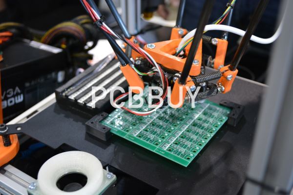
What is SMD soldering?
Historically speaking, we soldered SMDs by hand until the advent of pick and place machines. Because of their nature, SMD components are conducive to soldering.
They are perfect for first-time hobbyists who want to learn how to solder components to their PCBs. You can solder them traditionally, use solder paste, or flood with solder.
If machines do the soldering, the first machine in the process will be the solder paste printer. It applies the solder to the pad. After solder is applied, we perform an inspection.
Next, we surface to mount the components into the PCB pads. The PCB then goes through a pre-reflow automated optical inspection to ensure the integrity of the component placement process.
The PCB will go through the reflow soldering machine, forming the connections between the components and PCB. Finally, the PCB will go through post-reflow automated optical inspection.
Industry Category


