What is Slot in PCB and the Top 5 Factors of Manufacturing Process?
By:PCBBUY 12/06/2021 09:34

A PCB slot is a hole in the circuit board that is too big to be formed by normal drilling methods. Manufacturers need to cut out these holes with a routing bit during the fabrication of the PCB. A slot PCB can either be non-plated or plated. In this passage, you will learn more information about the slot in PCB. If you are looking for more information of slot in PCB, please check and read the content below in this passage.
1. What is the basic definition of slot in PCB?
If you are including slots in your PCB design, it is better to put them in Gerber mechanical layer. This layer is the safest way that shows the slots and the profile of the circuit board. There are two ways to do this:
· Use flashes or draws featuring the right end size of the slot
· Use a 0.50mm line to draw the slots. The line helps to analyze the clearance of the copper to the circuit board edge.
You can combine the slots’ definition with the PCB contour into the Gerber file. The mechanical layer must be with the copper layers. However, ensure the copper layer also features the PCB outline. If no mechanical layer is available, you may have to use another layer.
Don’t define slots in a legend layer or copper layer only. This is because they are easy to misunderstand. Indicate large cut-outs in a legend or copper layer. However, ensure you put a clear outline. Also, it is very important you indicate the slots in a README file. Do this when you are skeptical about the right one.
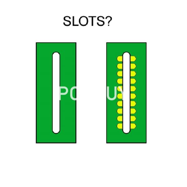
2. What are the plated-through slots?
Plated-through slots, metal slots, and cut-outs refer to the same technology in PCB manufacturing. A plated slot means a slot is plated with copper. Actually, the plated-through slot is the plated-through hole pads with non-circular shape. Circular plated-thorough holes are the ideal choice for most through-hole components. But there are many components with rectangular or blade-shaped leads, which need the plated-through slots. The process of plating the slot is the same with plating holes. First, to mill the slots, then do copper sink, and surface finish is the last step. And the slots have two kinds: plated-through hole (PTH) and non-plated through hole (NPTH).
3. How to define the slot in PCB?
If you want to add slots or cutouts in your design, putting them in Gerber mechanical layer is preferred. The safest and clearest way in a Gerber mechanical layer which shows the slots or cutouts and the profile of the PCB? Two possible ways forward:
· Use draws and/or flashes with the correct end size of the slot/cut-out.
· Draw the slots/cutouts with a 0.50mm line. It has the advantage that at the same time the line helps you to visually check the clearance of any copper to the PCB board edge. Our engineer will take the center of the line as the edge of the slot.
Combine your definition of the slots or cut-outs with the PCB contour (outline) into the Gerber file. This layer should line up with the copper layers, but to be as safe as possible make sure that the copper layer also includes the PCB outline. Different systems have different names for the mechanical layer. Provided that you have included milling in your order (see below) our engineers will find the right file.

4. What are the applications of slot in PCB?
Milling slots create air gaps for isolation of voltage on circuit boards
There can be temporary electrical arcs between traces in a circuit board featuring high voltages. Repetition of electrical arcs can result in PCB carbonation. This can cause a short circuit in the long run. As a result of this, PCB designers include a milling PCB slot between suspect traces.
Plated slots are ideal for parts featuring square or rectangular leads
These slots fit in for parts with square/ rectangular leads rather than the rounded ones. The footprint for slots is better than for large holes. This is because the space between the wall of the hole and the lead must contain enough solder.
5. How to show the plated-slots on the Gerber?
First, place copper pads on the top and bottom solder mask layers.Second, place the milling slot in the mechanical/contour layer.
· Plated holes/slots
The holes are with copper in the circuit layer, and holes have openings in the solder mask layer.
· Non-plated holes/slots
The holes are without copper in the circuit layer, and the openings don’t matter in the solder mask layer.
· Some applications for PTH/NPTH
· Plated-through slots are suitable for the parts with rectangular or square (rather than round) leads or pins, such as DC jacks.
· Milling slots are to form air gaps for voltage isolation on the PCBs.
In most PCB manufacturers, there are a lot of different footprints and component types for PCB assembly. Most through-hole part outlines are designed with round holes to accommodate round or square leads. This configuration is ideal for most through-hole assemblies, but many parts use rectangular or “blade” style leads and do not fit well into round or square holes. Therefore, using a plated slot package is a better choice.
Industry Category


