Solder Bridging in PCB
By:PCBBUY 08/18/2021 17:32

Solder mask as a very important process in PCB manufacturing, will affect the performance, appearance and quality of the finished products of PCB. And during the process, do you know solder bridging? How to avoid it? In this passage, we will focus on the solder bridging. If you are going to learn more information about it, come and check the content we prepare below.
If you want to order PCB product, please check and custom your order online.
What is the definition of Solder Bridging of PCB?
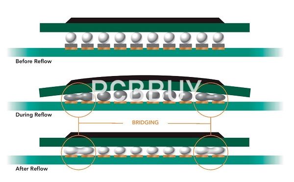
Solder Bridging is an issue that arises at the time of soldering. Solder bridging is defined as a defect under IPC-A-610D. It occurs when component pads on a PCB get connected due to the application of excess solder. Normally, each pad or component pin is intended to be separated from each other, but the occurrence of a solder bridge connects them and forms a conductive path between them, which can cause the component and thus the circuit to malfunction. Solder bridging is a microscopic phenomenon. Any solder bridge, which goes undetected during inspection, may cause a short-circuit in the component traces.
What are the causes of Solder Bridging of PCB?
Solder bridges can be caused by a lot of things, ranging from bad solder paste stencils or bad placement registration to messy assembly lines or clumsy rework techs.
Solder naturally wants to wick towards heated metal or other melted solder, and a lot of the printed circuit board assembly process relies on that fact. When solder reflows, it has a lot of surface tension, so it tends to stay balled up where it belongs and to hold things to it, nicely. Anything that disrupts that natural tendency can lead to bridging.
·Using too much solder on SMT pads because of an incorrect stencil specification.
·Having a bad seal between a stencil and bare board during the printing process.
·Designing solder pads that are too big in relation to the gap between pads.
·Placing components imprecisely or having a reduced component lead to pad size relationship.
·Having an insufficient layer of solder resistance applied between the pads on your board.
How to prevent Solder Bridging of PCB?
PCB designers can prevent solder bridging from occurring. It is better to prevent this mistake than to look for ways to correct it. Although PCB designers can’t control the assembly process, they can help to reduce the occurrence of this problem. Below are some methods that can help you to avoid solder bridging from occurring:
Apply solder mask properly
Improper application of solder masks can be another cause of solder bridging. A solder mask is used everywhere the solder is not wanted. During soldering, you apply a solder mask everywhere. It is important you apply it between the pins of the components. The risk of solder bridging can increase if the solder mask isn’t applied between the pins.
Use a high-quality PCB assembly House
Employing the services of a contract manufacturer might help you with the risk of this problem. A contract manufacturer that will keep you informed about their process is a good one to work with. You can make an inquiry to know their processes better. Ask questions about how they carry out the inspection processes on the board and how they develop their stencils.
Avoid mixing new and old flux for solder paste
For solder paste preparation, it isn’t ideal to mix new and old flux. Mixing new and old flux during soldering can increase the risk of solder bridging. Adhering to these rules will go a long way in helping you prevent solder bridging.
Utilize the appropriate pad diameter and hole size for through-hole parts
Solder bridging can be a result of extremely large holes or surface pads. A pad that is very large reduces the distance between the soldered surfaces. The reduction in the distance can cause Solder Bridge. It is, therefore, important to size the pad and plated it through hole correctly.
Utilize the appropriate lead lengths for through-hole parts
Solder bridges can result from through-hole components with very long leads. The appropriate lead length is determined by the size and thickness of your board. The type of soldering and the component size and mass will also determine the lead length.
Put fiducial marks on your circuit board
When you put fiducial marks on your boards, it will enable a machine to identify your PCB and arrange all the placements on each part of your PCB. According to the IPC, three fiducials should be used. Two marks in opposite corners and one mark in another corner. Utilizing poor fiducials will increase the risk of solder bridging.
Design for producibility
It is important to design for producibility. This will help reduce the risk of bridge soldering. According to the Association Connection Electronic Industries, Level A is the suitable level for overall producibility. You can’t avoid small spacing in some designs; however, they can be avoided in many designs. Don’t use unnecessary small parts.
Industry Category


