Thermal Relief PCB
By:PCBBUY 09/07/2021 09:16

Managing and conducting heat is important to PCB. Most circuit boards will have large areas of metal for power or ground planes, and those planes will typically connect to several component pins. And if you are looking for the professional knowledge about thermal relief PCB, welcome to check and read the content we prepare for more information.

What is the definition of thermal relief PCB?
In the area of PCBA, managing and conducting heat is essential to a circuit board's overall design success. Nearly all PCBs utilize large areas of metal for ground planes or power planes, and these planes will generally connect to numerous component pins. When these pins are the leads for a thru-hole device, unsoldering or soldering these pins can pose a high level of difficulty with the significant amount of metal in the planes. This brings about the need for thermal relief.
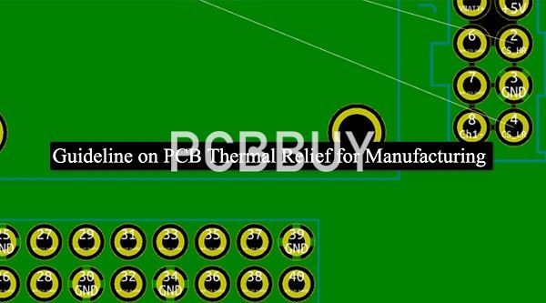
Thermal relief for a PCB comes in the form of a thermal relief pad or thermal pad. These thermal relief pads are PCB pads that are connected to a copper pour using a thermal connection. Whether your PCB design is a simple single-sided board or an intricate multi-layer board, there will usually be some significant areas of metal on it for power conduction and ground. The metal can be a network of traces, or maybe a sizable, filled power plane.
Thru-hole component pins
These pins may not get enough heat to solder correctly, resulting in a cold solder joint. Additionally, trying to unsolder a thru-hole that is soldered directly to large areas of metal could force too much heat to be applied to melt the solder. This excess heat could potentially damage nearby traces or components.
Surface mount component pins
Smaller two-pinned SMT parts may also have problems if one of their pins is trying to solder directly to a large area of metal. The unbalanced metal between the pins could result in the solder melting faster on one side than the other, pulling the part up and away from the other pin.

Why thermal relief PCB is important?
Thermal relief plays a vital role while creating your circuit design. You can use the thermal relief pad anytime when you connect the negative plane to the thru-hole part. You know that the thermal relief pad has a varying number of spokes with different width based on how much power requirements are needed for a pin. A power pin, requiring a 40 mil trace and connecting a plane, must have the pad with four 10 mil spokes.
However, the question is- Do your PCB vias need these thermal relief pads. The major reason for using this pad is to maintain a balance of the heat-sinking activities of pins soldered into planes. As the vias do not get the component pin, it does not need any relief pad with thermal properties. It will establish a link to the plane.
What are the guidelines of thermal relief PCB?
Are you going to deal with thermal relief PCB? Then, you must know some relevant guidelines to avoid mistakes.

· You have to use thermal pads while connecting your thru-hole pin to the power place, metal fill, and other bigger metals.
· You must know how much power the pin can conduct. Based on this factor, you can identify the width and number of spokes. You can achieve 40 mils of spokes with 4 spokes. Each of these spokes must have a width of 10 mils.
· SMT components directly soldered to the big metals must have some thermal relief between the metal and solder pad.
· In a few cases, you may not be able to connect all spokes to the thermal relief pad. The congestion of thermal reliefs can result in this problem. Moreover, when the metal has very limited space, and you use thermal reliefs in the split plane, you will encounter this problem. You have to ensure that the chosen software has its own rules to detect minimum connections of thermal reliefs.
· It is essential to know about the terminologies related to components and pads.
· Termination and termination width– Termination refers to a metallization band present at the chip component’s end. The termination’s width is about the dimension across the chosen component.
· Tolerance– It is about how much pad is used under your component.
· Overlap– The component termination covers a pad surface known as overlap. The overlap has a length that includes tolerance.
So, be sure to enlist the assistance of one of your company's greatest assets--your contract manufacturer. Be sure that your CM has the necessary experience in building the types of PCBs that match your company's needs. With heat management and thermal relief being vital to circuit design, ensure your CM understands the intricate details of proper thermal relief.
Industry Category


