What is Thermal Relief in PCB during the PCB Manufacturing Process?
By:PCBBUY 11/23/2021 10:03

Thermal relief for a PCB comes in the form of a thermal relief pad or thermal pad. These thermal relief pads are PCB pads that are connected to a copper pour using a thermal connection. Whether your PCB design is a simple single-sided board or an intricate multi-layer board, there will usually be some significant areas of metal on it for power conduction and ground. The metal can be a network of traces, or maybe a sizable, filled power plane.
In this passage, we will focus on the thermal relief for a PCB. And if you are going to learn more information of thermal relief for a PCB, please check and read the content below in this passage for professional knowledge.

Why to pay attention to thermal relief for a PCB?
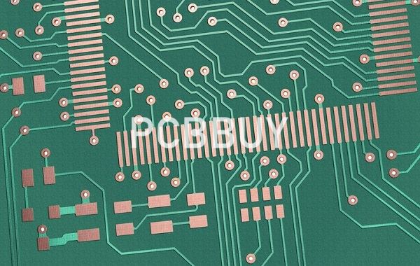
Thermal reliefs are the spooked connections from a thru-hole or surface mount pad to an area fill or plane. Their purpose is to provide a robust electrical connection from the pad to the plane while preventing the heat needed for soldering from dissipating into the metal plane. The green color represents a solid plane of copper on a circuit board in the picture below, and you can see four thermal relief connections for each outer pin. In the case of a surface-mount pin that connects to a large metal area, multiple traces may be used from the pad to the copper to accomplish the same results.
The purpose of the thermal relief is to aid in the manufacturability of the circuit board. While a direct flooded connection gives the best electrical performance, it also serves as a heat sink for pins connected to the plane. This sink could effectively pull the heat away from the pin during automated soldering operations and produce poor solder joints in the connection. Simultaneously, the heat sinking attributes of a direct connection would make manual soldering operations difficult for technicians during rework. Additionally, too much metal on one pad versus the other on small two-pin discrete parts can cause a thermal imbalance in the component. This imbalance can result in a manufacturing phenomenon known as “tombstoning.”
What are the considerations of thermal relief for a PCB?
A board's design dictates the component connections to these broad areas of metal for necessary functionality. One other exacerbating issue is that a design's requirements typically include as much metal as possible to accommodate the PCB's electrical demands.

And, to facilitate increased current loads and enhance power integrity, power nets also require this metal. As you might imagine, this creates a dichotomy between electrical performance and standards of manufacturability. However, this is where thermal relief can provide a much-needed compromise.
What is thermal relief pad?
Thermal relief is a technique used by PCB manufacturers to thermally separate soldering pads from large copper areas, to prevent excessive heat transfer from the pads during the soldering process, which would result in delayed melting of the soldering alloy or even no melting at all.
To know more about pad design read our article what is a Pad in PCB Design and Development? In the figure given above, there are two kinds of pads that are immersed in a copper pour. Figure A shows a conventional pad that is connected to a copper pour in all directions. Figure B shows the pad is connected to the copper pour through four spokes or traces. This is a thermal relief pad.
Even though this technique is a clear requirement from a manufacturing standpoint, designers exercise caution when using it. This is because thermal relief brings about concerns regarding the under-utilization of heat transfer capability of large copper areas. This might lead to localized thermal hot spots at component terminals.
Thermal management of your PCB involves several aspects such as the design of power planes, trace routing, via placement, and thermal relief pads. Mastering these aspects as a designer will ensure a more efficient and reliable PCB design.
How to design thermal relief for a PCB?
Electronic components become smaller and smaller every year; the market, in turn, demands electronics with ever-shrinking form factors. PCBs with dimensions under an inch are commonplace, and their surfaces are growing more tightly packed with placements. Some designers, in the interest of squeezing slightly more space out of a small area, are leaving out thermal reliefs — but this can be a bigger mistake than it seems.

A thermally relieved pad is an SMT pad with the copper around it removed (“relieved”) except for 2–4 traces. Adding thermal relief to pads that will have components soldered to them is crucial in directing and controlling the flow of heat through your board during reflow. Pads with poor thermal relief may not heat evenly in the reflow oven and cause tombstoning, no-connects, or poor solder joints, which require manual rework. Rework is then impeded by a lack of thermal relief as well. Adding thermal relief to your design can reduce quality problems as well as the time needed to repair them.
The use of thermal relief for these pads will make rework easier and quicker by eliminating the higher conductivity and time it takes to heat up all or most of a copper pour, as with a solder mask defined pad. A single pad with thermal relief will reach the correct temperature much more quickly. If there are component pads next to each other that share the same copper pour, it can be very time-consuming to heat up a pad, even for experienced technicians. In some cases rework may not be possible due to the amount of heat and time it takes to bring a pad up to temperature without thermal relief — components and/or the board’s surface can easily suffer damage from the extended use of a soldering iron. Thermal relief for pads is easy to implement, and strongly recommended for any electrical component that doesn’t require a high voltage current. With higher copper weights, thermal relief may save hours of rework time and also help ease the initial soldering process.
Industry Category


