What is Tooling Hole with PCB Component Placement Guidelines?
By:PCBBUY 11/27/2021 09:24

PCB tooling holes, or mounting holes, are circular openings made at the edge of a PCB. Tooling holes are non-plated, and they are used by machines to hold the PCB down for alignment. During the fabrication process, it’s imperative that the PCB be kept still and properly aligned for drilling. If the PCB is not kept still, it will be impossible to deliver precisely-drilled holes.
Do you know what is tooling hole in PCB? If you are going to learn the basic information of tooling hole in PCB, please check and read the content below in the passage for more information.
What is the basic information of tooling hole in PCB?
PCB tooling holes, or mounting holes, are circular openings made at the edge of a PCB. Tooling holes are non-plated, and they are used by machines to hold the PCB down for alignment. During the fabrication process, it’s imperative that the PCB be kept still and properly aligned for drilling. If the PCB is not kept still, it will be impossible to deliver precisely-drilled holes.
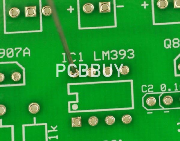
When the fabricated PCB is sent for assembly, the tooling holes will be needed again if there are SMD components in the design. The machines will use the tooling holes for stencil alignment when applying solder paste and placing SMD components with the pick-and-place machines.
How to determine the right size for tooling hole in PCB?
Usually, common sizes like 1mm, 1.5mm, and 2mm are acceptable tooling hole sizes for most manufacturers. If you’re unsure, make sure to consult with your PCB manufacturer. For uniformity, you’ll want to stick with a common size for all tooling holes on a PCB.
Besides size, you’ll also need to ensure that the PCB tooling hole isn’t plated. A non-plated hole is better in terms of accuracy compared to a plated one. Also, ensure that there is a solder mask expansion that slightly extends over the hole.

How to work with tooling hole in PCB?
Tooling holes will probably be one of the simplest features in your PCB, but they are critical for fabrication and assembly. There are three main points to consider when determining where and how to place tooling holes in your PCB:
· Placement during panelization
· Size and plating
· Placement with fiducials
What is the importance of tooling hole in PCB?
In addition to having leads or pins that solder to the circuit board, several components have mounting hardware for added physical support. Connectors often bolt to the board to protect their solder connections from the stress of being plugged and unplugged from their cable. Other components that are heavy or serve as interfaces may also be bolted down—including switches, fans, batteries, and speakers. These holes may also need to connect the mounting hardware to electrical ground or conduct heat through the board to be dispersed on interior plane layers. Lastly, to mount a circuit board into its system, mounting hardware or brackets are often attached to the board using isolated holes.
PCB tooling holes can be put into the board to assist with the different phases of manufacturing. These holes guide the board through its assembly processes, such as solder reflow, wave solder, and automated optical inspection (AOI). Tooling holes are also used during the testing process if the board needs additional test fixture support. However, most of the tooling holes for production are added to the PCB contract manufacturer’s panel based on their requirements instead of the board.

How to process tooling hole in PCB?
Usually, common sizes like 1mm, 1.5mm, and 2mm are acceptable tooling hole sizes for most manufacturers. If you’re unsure, make sure to consult with your PCB manufacturer. For uniformity, you’ll want to stick with a common size for all tooling holes on a PCB.
Besides size, you’ll also need to ensure that the PCB tooling hole isn’t plated. A non-plated hole is better in terms of accuracy compared to a plated one. Also, ensure that there is a solder mask expansion that slightly extends over the hole.
PCB fabricators use them for aligning the board during drilling and routing. Assemblers use them
for alignment with stencils during solder paste printing, and for location on pick-and-place machines. They are used for alignment on electrical test fixtures. They may also be used as alignment holes in the final enclosure, often mating with small moulded plastic posts.
For some of these purposes tooling holes can be placed in the overall panel, but for activities that
occur after de-panelling, or for boards that are not panelised, tooling holes are required within
the board outline.Tooling holes are often standard sizes, for compatibility with commonly used locating pins.
Common imperial sizes are 0.062", 0.093" and 0.125". Common metric sizes are 1.0mm, 1.5mm,
2.0mm, 2.5mm and 3.0mm. Tooling holes are always un-plated. This gives better accuracy since plating thickness is not well controlled.
Industry Category


