PCB Via Stitching
By:PCBBUY 08/21/2021 09:51

Do you know what is Via Stitching in PCB?If you are looking for more information about it, please check and read the content below to learn the knowledge. Let’s go!
What is the definition of via stitching?
Via stitching is a technique used to tie together larger copper areas on different layers, in effect creating a strong vertical connection through the board structure, helping maintain a low impedance and short return loops. Via stitching can also be used to tie areas of copper that might otherwise be isolated from their net to that net.
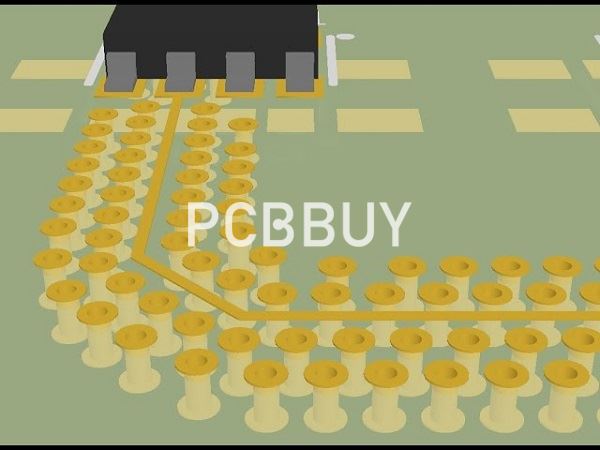
What are the main types of PCB via stitching?
A via stitching is a process where multiple numbers of vias are used to drill the copper areas on different layers and then connected. It is generally done on the larger copper planes, such as Ground filling planes, Power planes, etc.
For example, there are different types of Via stitching processes available in the PCB design that are different from others but at the same time, it is the same in terms of the concept. The different Via stitching can be summarized as:
· Constant Ground Via stitching
· Thermal Via stitching
· Shielding Via stitching
How to add via stitching on PCB?
The via stitching algorithm treats Polygons, Fills and Planes in the following way:

· Polygons and Fills that are on the same net are stitched wherever they overlap on different layers. If there are Polygons or Fills on other nets that are overlapping within that area (on another layer), stitching is not applied in that region. Overlapping Plane regions on other nets are passed through.
· Overlapping Plane regions on the target net are always stitched, regardless of the presence of Plane regions (on another layer) attached to other nets. Rule 1 above applies if there are Polygons or Fills overlapping in the same region.
· Configuring the Stitching Parameters
Notes about the Add Stitching on PCB:
· Select the Net to be used for stitching first as this effects the behavior of other options, such as clicking the Load values from Routing Via Style Rule button.
· The Grid is the distance between the centers of adjacent stitching vias and applies in the X and Y directions. Stitching vias will not be placed in violation of applicable design rules if a potential via site would result in a violation, that site is skipped.
· If the Stagger alternate rows option is enabled, alternate rows of stitching vias are offset by half of the Grid value.
· The Same Net Clearance options control the clearance between stitching vias and vias and pads on the same net. There are two ways of controlling the clearance between same-net objects.
· The stitching Via Style can be configured manually, or it can be selected from those available in the Template dropdown.
What are the considerations of via stitching on PCB?
Here are some other high current layout considerations to keep in mind as you are planning out your design:

· PCB fabrication: If your board is going to be running very hot with high current, it may be best to explore other materials that can handle a higher operating temperature. Although these materials may be more costly, they may end up saving you expenses in the long run by avoiding thermal-related problems. You should also work together with your manufacturer to develop the best layer stackup configuration and power plane strategies for your high current board as well.
· Board thickness: By increasing the thickness of the board you can increase the weight of the copper giving you a thicker trace. This may allow you to decrease the trace width, allowing for more routing and component placement room. As with any fabrication issues, these changes should be agreed upon with your manufacturer before you include them in your design.
· Automated assembly: As we have seen, higher currents require more metal for electrical and thermal reasons. At the same time though, the same metal that is dissipating undesirable heat during operation may also create problems for PCB assembly. Large areas of metal can create thermal imbalances for smaller parts that can affect their soldering. To avoid this, make sure to use thermal reliefs when connecting parts directly to wide traces or large areas of metal.
· Component placement: Parts that carry high currents and run hot should not be placed on the edge of the board if it can be avoided. By placing these parts more towards the center of the board, there is greater room for the heat to be naturally dissipated by the board.
Industry Category


