What is Via in Pad in the PCB Manufacturing Process for Beginners?
By:PCBBUY 11/08/2021 10:23

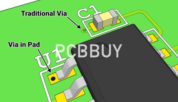
Via in pad helps to reduce inductance, increase density and employ finer pitch array packages. The via in pad approach places a via directly under the device’s contact pads. This allows higher component density and improved routing. Consequently, via in pad provides the designer significant PCB space savings. For example, traditional fan-out places four components, whereas with via in pad, six components can be placed within the same board outline.
If you are interested in the topic of via in pad of PCB, please check and read the content below for more information.
How to design via in pad of PCB?
Via in pad is the design practice of placing a via in the copper landing pad of a component. Compared to standard PCB via routing, via in pad allows a design to use smaller component pitch sizes and further reduce the PCBs overall size. With component manufactures pushing smaller parts every year and the demand from consumers for smaller devices, the usage of via in pad practices by hardware engineers have become more commonplace. In this article, we will discuss the differences between via in pad and traditional vias, when should you use via in pad, and how to design for it.
What are the advantages of via in pad of PCB?
Amongst other things, this faciliates additional conductor traces for BGAs (marked red in the picture).We use this technology for years now and know how to ensure a reliable and safe production process.
Additional advantages:
· Improved thermal dissipation
· Increased voltage capability of the via
· Provides a flat, coplanar surface
· Lower inductance due to no dog-bone pads with traces
How to route via in pad of PCB?
The most compelling reason to use via-in-pad routing for your SMDs is space. Either your board size is limited, surface routing options are restricted or your design components have very small connection points (pads or balls) and other routing options are inadequate to accommodate your need for reduced space. Although size requirements alone can be compelling enough to consider via-in-pad routing, there are other advantages for your board as well.

Compared to other options, via-in-pad involves easier routing for big or fine pitch BGAs (which can be smaller than 0.75mm). Without surface routing from your SMD, you can place bypass capacitors very close to the components, minimizing inductance. This is highly recommended to promote better thermal management. There is no need for via-plugging (i.e. sealing open vias that may draw solder during assembly) since the vias are located directly under the component. Via-in-pad routing is also helpful for high-frequency component grounding.
Although advantageous in various situations, via-in-pad routing comes at a price. You have to ensure that your manufacturer can eliminate surface bumps, which can complicate the process of attaching components like BGAs. However, the primary disadvantages of utilizing via-in-pad technology are increased complexity and additional material cost for conductive fills. Creating and filling extra vias adds steps to the fabrication process, such as:
· Drilling additional holes;
· Plating the vias with copper or another conductive material;
· Filling the plated vias with epoxy; and
· Covering or capping the vias with copper.
What are the common issues via in pad of PCB?
The primary reason we don't want to see vias in pads is that when left open, those via holes act like little capillary straws and suck solder off of the pad. A couple of undesirable events can happen, depending on the method used during board fab:
If your vias are left open, solder will tend to wick down into the via hole. The larger the diameter, the worse the wicking problem can be. You might end up without enough solder left to secure the component, or even a solder bump on the bottom side of the board that could interfere with other components or lead to shorts.
If your vias are capped or partially filled, the caps might pop off due to thermal expansion or out-gassing. Internal air bubbles can migrate up, leading to voids in your solder joint.
Open vias in pads are not an industry-accepted practice. In a perfect world, we'd like to never see one. However, the real world is saying otherwise. Manufacturers of QFN parts are starting to recommend vias in the heat-slug pad for improved thermal conductivity. High-frequency designs benefit from the shortest possible routing, which may indicate via in pad. Super-fine-pitch BGAs may not leave any other options.
Industry Category


