Gerber file extension
By:PCBBUY 08/06/2021 09:12

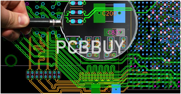
A Gerber, or Gerber Extended File, is a standard file format used in the electronics industry to store and communicate design blueprints. They're often used to convey information regarding manufacturing specifications of printed circuit boards. At their core, Gerber files are like PDFs for electronics manufacturing industry. Have you ever gone through an X-ray inspection in a hospital when you suffered from a fracture of bones? You can totally imagine a Gerber file as an X-ray image of a real PCB. An X-ray image just tells how your bones are organized while a Gerber file indicates how circuits are led in a PCB.
In this article, we are going to provide everything about Gerber file extension, please check the content below for more professional knowledge.
How does Gerber extension file work?
So how are Gerber files used in PCB manufacturing? In the subtractive method of PCB manufacture, the PCB starts as a sheet of substrate material encased in copper on one or both sides. Gerber files are used to provide a picture of where the multilayer PCB copper should remain at the end of the process.
The picture is then used to guide the creation of channels to remove copper from the board to leave only the conductive traces used by the actual PCB. The standard convention is to use clear markings for areas with no copper and black markings for the actual copper traces. But it doesn't stop there. Once the copper traces are marked out, layers like the solder mask and silkscreen cover them. The Gerber file will also have pictures for these other layers, representations of locations of the board's drill holes and even a designation of the board's size.

Since Gerber files contain so much info, PCB Houses get up to 9 files - although they're making just a two-layer PCB. Examples include:
• The copper traces for the top of the circuit board
• The copper traces for the underside of the circuit board
• A picture of the solder mask for the top layer
• A picture of the solder mask for the bottom layer
• Silkscreen imaging for the top layer
• Silkscreen imaging for the bottom layer
• The coordinates of all drill holes, as well as their properties
• An outline of the physical board with all the machining operations marked out, such as scoring, slots and internal cutouts
• A simple text README file explaining the uses for all files
What is the post-design process of Gerber file extension?
Multiple software applications lead to different methods to create Gerber files, including Cadence and Altium Designer. After design, a photoplotter transfers the Gerber to the PCB. The photoplotter prints out each of the files on one piece of film.
Each PCB layer and the accompanying solder mask gets its own sheet, so a simple two-layer PCB needs a minimum of four sheets of film - one each for the top and bottom trace layers and one each for the accompanying layers of solder mask.
After printing, the photoplotter punches a "registration hole" through the lined-up films. The registration hole is used as a guide to align the pieces of film onto the copper and substrate layers, so the film covers the substrate panel.
A photo-sensitive film consisting of a layer of ultraviolet-hardened chemicals then covers the PCB blueprint. Known as a "resist," this film allows the PCB manufacturer to receive a perfect match for the photos on the Gerber file.
Once the resist and the layer of substrate have been lined up using the registration holes from earlier, they receive a blast of ultraviolet light that passes through the translucent parts of the film, hardening the photo resist. This indicates areas of copper trace that are meant to remain as pathways. In contrast, the black ink prevents any light from getting to the areas that shouldn't harden so they can later be removed.
This process repeats for each layer, including the solder mask layers and the silkscreen layers. When it comes to designing a Gerber file and transferring to a PCB, there are two considerations designers need to consider.
1. Legacy Issues
Gerber file format was originally used to drive numerically controlled photoplotters. Today's PCB printers are much more in line with a modern laser printer - something the Gerber file format wasn't built to handle, which causes issues when the files are used with current raster plotters to print PCBs:
• Hole data can be absent because the original photoplotters used for PCB manufacture didn't drill holes. Excellon numerical control files can be used to augment the Gerber data, but even this is incomplete - it doesn't differentiate between through, blind or buried holes. Technicians reading the data also have no idea whether they are offset correctly or using the correct scale.
• No functional definition or mapping of the files. Nothing in the Gerber file itself tells the CAM technician whether it's a top, bottom or mirrored file. This is why most current Gerber files include a README.
2. Design for Manufacture (DFM) Issues
Gerber files contain no way to read the "intent" of the PCB. There are also no protections against a PCB designer building a PCB that is difficult or even functionally impossible to create. One of the most common errors that PCB technicians need to watch out for is missing files, but other errors include:
• Putting silkscreen onto the PCB pads
• Putting features of the PCB too close to the outline of the PCB
• Drilling holes twice, making them unnecessarily large
<Industry Category


