What is a PCB Interconnect in PCB Design for Beginners?
By:PCBBUY 12/28/2021 09:54

As a part of the whole machine, a PCB generally cannot constitute an electronic product, and there must be the problem of external connection. For example, electrical connections are required between PCBs, PCBs and components, PCBs and panels of devices, etc. Therefore, the choice of the best interconnection which combines reliability, manufacturability, economy in one is one of the most important contents in PCB design. There are different kinds of the methods of interconnections that we’re free to choose on base of the different characteristics of different interconnections.
Are you a beginner of PCB industry? In this passage, we are providing all the professional knowledge of PCB interconnects. If you are looking for the information of PCB interconnects, please check and read the content below.
What are the considerations of PCB interconnects in design?
While true that a multi-board solution may not be the optimal approach in terms of functionality, there are reasons why you have to use this approach.
It could be something as simple as accommodating for a strict form factor or the need to easily isolate power or sensitive signals. You may be charged with using an “off-the-shelf” board to talk to specific components or a custom board (such as LCD displays). Other reasons for stacking boards could include designing for future expansion (like the common Arduino shields), having multiple design configurations (maybe a basic version and an advanced version) or just making your design modular in general (a sort of mix-and-match).
There will be some bumps in the road, but if you stick to a good plan and employ sound principals to reduce common pitfalls and risks, the final printed circuit board, PCB interconnect(s) and application will reflect that same level of quality preparation.
Partnering with an experienced PCB manufacturing and assembly provider with engineers that have worked with and modified multiple layouts in preparation for fabrication and assembly of electronic interconnects is crucial for complex projects.

What are methods of process PCB interconnects?
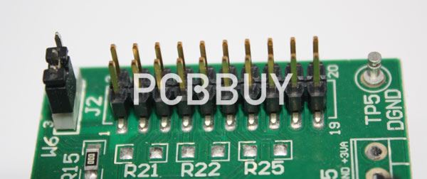
In more complex instruments and equipment, the interconnection methods of connector clip is often used. This "building block" structure not only ensures the quality of mass production, but also reduces the cost of the system and facilitates debugging and maintenance. When device fails, maintenance personnel do not have to check to the component level that is, in order to check the cause of the failure, until check to the specific component. This work will take quite a long time.), as long as maintenance personnel judge who PCB is abnormal, they can immediately replace that PCB, which cannot only eliminate faults in the shortest time, but shorten the downtime. Thus, it can improve the utilization rate of the device. In addition, the replaced PCB can be repaired in plenty of time and used as spare parts after repair.
This interconnection is often used in more complex instruments and devices. This method makes the printed plug from the PCB edge, and the plug part is designed according to the size of the socket, the interconnection points, the contact distance, the location of the positioning holes and so on, so as to make it match with the special PCB socket.
When manufacturing PCB, the plug part needs to be gold-plated to improve wear resistance and reduce contact resistance, which has the simple assembly, great interchangeability, good maintenance performance, and is suitable for standardized mass production. The disadvantage of this method is that the cost of PCB is increased, and the requirements of PCB manufacturing precision and process are higher. In addition, its reliability is poor. For example, it often lead to poor contact because the plug part is oxidized or socket spring aging. In order to improve the reliability of external interconnection, the same outgoing line is often drawn out in parallel through the contacts on the same side or both sides of PCB.

What are the advantages of PCB interconnects?
There are many of types of PCBs to choose from when doing prototyping, ranging from simple one-sided PCBs to incredibly complex, multi-layer boards. Generally, the most simple prototype printed circuit boards are the ones that contain copper tracks, or interconnections between its components on only one of its surfaces. These boards are known as one-layer printed circuit boards, or single sided PCBs.
· These PCBs are extremely compact. Considering that HDI PCBs have a higher wiring capacity, they are one of the best options for engineers looking for the smallest circuit board with the largest output. HDI capacity makes it easier to turn a 10 layered PCB into a four or five layered one, which is great for those looking for smaller boards without skimping on quality. Since most consumers prefer small devices, this can be a huge design advantage.
· The ability to place more components on one side. These HDI PCBs utilize blind and buried vias, and Via-in-Pad technology, as methods of placing components closer together, which results in faster signal transmission. Making it an ideal technology for RF circuits.
· Laser drill technology makes PCBs into advanced electronic circuits. This manufacturing technique allows for smaller holes to be used and gives the board higher heat resistance.
Industry Category


