What is a PCB Panel?
By:PCBBUY 05/28/2025 16:37
Introduction: The Essence of PCB Panels
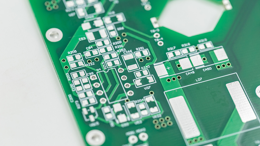
A PCB panel refers to a large, multi-unit assembly of printed circuit boards (PCBs) fabricated as a single entity. This process, known as panelization, is a cornerstone of modern electronics manufacturing, enabling cost efficiency, high precision, and scalability. By grouping multiple PCB units into a single panel, manufacturers optimize material utilization, reduce defects, and streamline production workflows. This article explores the technical foundations, manufacturing processes, and industry applications of PCB panels, supported by data from IPC standards and leading manufacturers like PCBBUY .
1. What is a PCB Panel?
1.1 Definition and Purpose
A PCB panel consists of multiple individual PCB units connected via tabs (small bridges) or routing channels. These units are later separated (depaneled) for use in electronic devices. Panelization allows manufacturers to:
-
Maximize yield: Edge defects are distributed across the panel, reducing per-unit waste.
-
Lower costs: Shared tooling (e.g., drilling, plating) reduces per-unit expenses by 30–50%.
-
Enhance precision: Registration accuracy of ±0.05 mm ensures consistent layer alignment.
1.2 Key Components of a PCB Panel
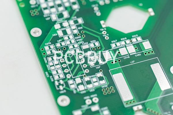
|
Component |
Function |
|
Substrate |
Provides mechanical support and electrical insulation (e.g., FR4, high-Tg materials). |
|
Copper Foil |
Conducts electrical signals; typical thickness: 1 oz/ft² (35 μm) for signal layers. |
|
Solder Mask |
Protects copper from oxidation and prevents short circuits. |
|
Silkscreen |
Marks component locations and identifiers for assembly. |
|
Tabs/Routes |
Connect units during panel processing, later milled or broken apart. |
2. Why Panelization Matters in PCB Manufacturing
2.1 Advantages Over Single-Board Production
|
Metric |
Single-Board Production |
Panelized Production |
|
Material Utilization |
60–70% (edge scrap losses) |
>90% (minimized scrap) |
|
Defect Rate |
~8% (higher risk per unit) |
~2–3% (redundancy mitigates edge issues) |
|
Cycle Time per Unit |
10–15 min |
2–3 min (batch processing) |
|
Thermal Stress |
High (individual curing) |
Low (uniform heating/cooling) |
2.2 Industry Standards for Panelization
-
IPC-2581: Standardizes panel design files, including tab dimensions and breakaway margins.
-
IPC-6012: Specifies coating requirements for solder masks and finishes.
3. Design Considerations for PCB Panels
3.1 Array Layout and Tab Routing
-
Array optimization: Units are arranged to balance panel symmetry and minimize warping.
-
Tab design: Small copper bridges (0.2–0.5 mm wide) connect units, ensuring electrical continuity during fabrication.
-
Breakaway margins: At least 0.5 mm gap between units to prevent solder overflow during separation.
3.2 Material Selection
3.2.1 Substrate Materials
|
Material Type |
Dielectric Constant (Dk) |
Thermal Resistance (Tg) |
Key Applications |
|
FR4 |
4.2–4.8 |
130–170°C |
General electronics, low-frequency |
|
High-Tg FR4 |
4.2–4.8 |
>180°C |
Automotive, industrial controls |
|
Rogers RO4350 |
3.45 |
280°C |
High-frequency RFID, 5G basestations |
|
Isola TLC |
3.0–3.2 |
250°C |
Medical devices, aerospace |
3.2.2 Copper Foil and Lamination
-
Copper weight: 1 oz/ft² (35 μm) for signal layers; 2 oz/ft² (70 μm) for power planes.
-
Lamination parameters: 350–400 psi pressure at 175°C for FR4, ensuring <5% void density.
4. The PCB Panel Manufacturing Process
4.1 Inner Layer Processing
-
Dry film coating: 20–30 μm photoresist applied to inner layers.
-
Exposure: UV light patterns vials with ±0.05 mm alignment tolerance.
-
Etching: Ferric chloride solution removes unwanted copper, targeting ±0.05 mm line width.
4.2 Multilayer Lamination
-
Alignment: ±0.075 mm registration across stacked layers.
-
Post-lamination cooling: Controlled at 2–5°C/min to prevent thermal stress.
4.3 Outer Layer and Surface Finish
-
ENIG (Electroless Nickel/Immersion Gold): Deposits 2–5 μm Ni and 0.05–0.15 μm Au for solderability.
-
Laser drilling: Microvias with diameters down to 0.1 mm (tolerance ±0.01 mm).
5. Advanced Techniques in Panelization
5.1 High-Density Interconnect (HDI) Panels
-
Ball grid array (BGA) support: Pad pitches down to 0.4 mm for fine-pitch components.
-
Embedded passives: Resistors/capacitors integrated into layers to save space.
5.2 Thermal Management Strategies
-
Coefficient of Thermal Expansion (CTE) matching: Ensures layer-to-layer stability within ±5 ppm/°C.
-
Thermal vias: Copper-filled holes that dissipate heat from high-power components.
6. Quality Control and Common Challenges
6.1 Inspection Protocols
-
Automated Optical Inspection (AOI): Detects missing pads, shorts, or opens with >99% accuracy.
-
X-ray imaging: Verifies inner-layer connectivity (minimum hole size: 0.2 mm).
6.2 Challenges and Mitigations
|
Challenge |
Root Cause |
Solution |
|
Microvia cracking |
Thermal coefficient mismatch |
Use resin-rich capillary layers |
|
Solder mask bridging |
Stencil misalignment |
Laser direct imaging (LDI) |
|
Interlayer delamination |
Adhesion failure |
Add silane adhesion promoters |
7. Applications of PCB Panels
PCB panels are ubiquitous in industries requiring high reliability and scalability:
-
Automotive: Engine control units, advanced driver-assistance systems (ADAS).
-
Medical: CT scanners, portable diagnostic devices.
-
Telecommunications: 5G basestations, network routers.
-
Consumer Electronics: Smartphones, wearables, IoT devices.
8. Future Trends in PCB Panelization
-
Additive manufacturing: Hybrid panels combining traditional etching with 3D printing.
-
AI-driven design: Machine learning optimization for panel layout and defect prediction.
-
Sustainable materials: Bio-based laminates and recyclable copper foils.
9. Conclusion: The Backbone of Modern Electronics
PCB panels are the linchpin of efficient, high-volume manufacturing. By leveraging advanced materials, precision processes, and rigorous quality control, manufacturers deliver reliable PCBs for diverse applications. As technology advances, innovations in panelization will continue to drive miniaturization, performance, and sustainability in electronics.
References
-
IPC Association. (2023). IPC Standards Handbook.
-
Prismark Partners. (2022). Global PCB Industry Report.
-
Rogers Corporation. (2021). High-Frequency Laminate Datasheets.
-
Isola Group. (2023). Thermal Management in PCBs.
-
JLCPCB. (2025). Technology Capabilities: High-Layer PCB and Panelization.
Industry Category


