PCB file
By:PCBBUY 05/25/2021 17:46

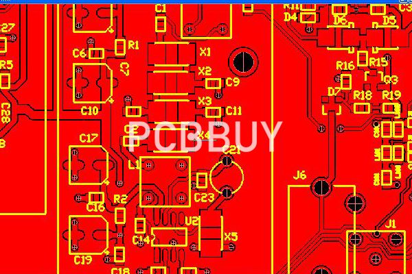
PCB files contain the application settings and data that are used by the software. The pcb file contains the necessary information on layers and other stuff related to the printed circuit board. The file contains information on every layer and routing on that layer. And it also contains information related to the top and bottom silk screens and hole sizes.
For complete electronic product design, proper planning and designing are required. The digital software on the computer gives the flexibility to simulate the designed circuit. And omit the errors before it gets fabricate. But a deep understanding of the course and powerful software to make it simulation gives an error-free design.
After finalizing the design, the appropriate selection of making components, the footprints of these components are available in the software. Also, it becomes part of the PCB board file when making the final print—and finishing the wiring connection and optimal routing in the software based on the footprint of placed components on different layers and the surface of the board.
The appropriate power points and signal traces plan is generated and digital software on the computer gives an output of a designed, printed circuit board. This designed circuit board is in the form of a Gerber file or a PCB file.
What Are the Common Problems of a PCB File?
Printed circuit boards are a crucial element for a wide variety of businesses, especially now in the digital age, when electronic technology is so important to many different fields. There is a significant range of different types of printed circuit boards as well, with different materials, shapes and sizes depending on the needs of a particular company or industry. PCB designers are constantly trying to find ways to develop circuit boards that are faster, stronger and more efficient.
One thing all of these printed circuit boards and PCB designs have in common, however, is their reliance on quality Gerber files. Gerber files are the digital blueprints of your PCB, the layer-by-layer input for the PCB manufacturers that detail the manufacturing and fabricating process. Gerber files mistakes can be disastrous for a PCB manufacturer, leading to PCB manufacturing errors and printed circuit boards that fail prematurely or do not work at an optimal level.
Avoiding Gerber files problems so that these files are complete and accurate is critical to making sure each printed circuit board comes off the line able to perform according to specifications. Here are some of the most common Gerber file issues PCB manufacturers encounter and what they can do about them.
Empty Gerber files
Believe it or not, it is possible for the designer to create Gerber files with no information in them, or “zero-byte” files. Whoever is reading the file will not know if the file is completely extraneous or if there was information in it that was accidentally deleted. Designers must check each Gerber file to make sure it contains useful information before sending it on.
Missing or incomplete files
This is almost the opposite problem. Manufacturers need to know each specification related to the printed circuit board, from the size of the plated-through holes to the dimensions of the board. Any missing information will lead to a board that does not match the desired specifications. It’s important to make sure each necessary Gerber file is in place and accessible.
Bad file labeling
While not a catastrophic error, it is highly recommended that the designer name all Gerber files according to an established naming protocol the manufacturer understands. This way, the manufacturer can immediately find the Gerber file he or she needs without any confusion as to whether or not they have the right file.
Too many aperture lists
The Gerber files should ideally have a single aperture list with all the details the manufacturer needs about the tools they require for each stage of fabrication. Multiple aperture lists create confusion, can slow down manufacturing and may increase the chances of error. Also look out for designers who create aperture lists in a different format than the Gerber files, which can lead to confusion as well.
Composite layer design errors
If the designer’s software creates composite layers while generating individual layer design specifications, it’s important that the images are combined in a way that creates one Gerber file for each layer, to avoid errors.
Of all the potential problems you may have with your printed circuit boards, Gerber file mistakes are the most inexcusable. While most PCB design errors can be avoided with more careful and focused work, Gerber file errors are the easiest to avoid. Given that the consequences of Gerber file issues can be so expensive and so time-consuming, you simply cannot allow them to happen. A few ways to help you avoid Gerber files problems include:
1. Using a Gerber file viewer to check the Gerber files
2. Printing a sample board to make sure the specs are correct
3. Using high-definition CAD software
4. Following best QA practices throughout the design process
Industry Category


