PCB trace
By:PCBBUY 05/06/2021 18:03

There are many components in the PCBs and it is necessary to understand all the parts and materials as repairing or assembling the printed circuit board.
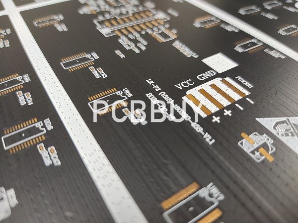
When we are talking about PCBs, trace is mainly in referring to the network of copper, wiring, insulation, as well as fuses that is made up of the board. In general, there is a high probability that the PCB trace is inconsistent if it has some wrong with any given electronic device. Besides, trace resistance is the most common term used by electronic engineers in the printed circuit board industry. As well as the trace resistance means the parts of a PCB that resist the flow of a current.
PCB trace is a really essential part for each PCB like a current, and it will spend more time and energies on fitting if make it wrong to detect or calculate the trace. On the contrary, it may lead to making mistake in the system for any device.

What is PCB trace thickness?
The thickness of a PCB board makes a great influence for a designer during the design process of a PCB board. The thickness holds essential gravity as by ignoring it the PCB board might not function or may result in damage or sparks which might also cause harm to the components connected to the board.
For electronic designer, the thickness of PCB plays an important role in the PCB design. The thickness can keep the balance, however, there will not function or lead to damage for the circuit board, as well as involving the components connected to the board. Because single-sided, double-sided and multi-layered PCB boards exist in the market so does the thickness of these boards also varies with the type of PCB board. And there are some common PCB trace thickness ranging from 0.008 inches to 0.240 inches, such as 0.2 mm, 0.4 mm, 0.5 mm, 0.6 mm, 0.8 mm, 1.0 mm, 1.2 mm, 1.5 mm, 1.6 mm, 2.0 mm, 2.3 mm and so on.
The significance of PCB thickness is equal if not less than that of a PCB board. The PCB thickness holds of immense importance. The designers perform a lot of complex calculations to reach the depth of PCB board that could deliver accurate results. In case of wrongly calculating the PCB trace thickness, this may result in either not gaining the accurate results that the PCB designed for or it may also result in damaging the components attached to the surface of the PCB board. Due to the accuracy of the PCB trace thickness material used during the design of PCBs is saved to avoid wasting or over-using.
What is PCB trace width?
There are several factors that drive trace width, length, and style during the PCB design process of the next PCB prototype. This article will dive into a variety of applications that demand specific trace layout characteristics and how to incorporate them into your PCB design.
So we are talking about the basics. What exactly is trace width and why is specifying a particular trace width so important? The point of a PCB trace is to connect any kind of electrical signal, whether it is analog, digital, or power, from one junction to another.
The junction can be the pin of a component, a branch off of a larger trace or plane, or an empty pad or test-point intended for probing. Trace widths are often measured in mils, or thousands of an inch. A standard trace width for an ordinary signal may be in the 7-12 mil range and be as long as a few inches, but there are many things that should be considered when defining the width and length of a trace.
The application will often drive the trace widths and types in a PCB design and at a certain point, there is usually a balance with regards to PCB fabrication cost, board density/size, and performance. If a board has specific design requirements such as speed optimization, noise or coupling mitigation, or high current, the trace widths and types might be more important than optimizing for manufacturing cost of the bare PCB or overall board size.
What is PCB trace spacing and length?
For digital designs with high speed communication, specific spacing and tuned lengths may be required to minimize cross-talk, coupling, and reflections. Some common applications for this are USB-based serial differential signals, and RAM-based parallel differential signals. Generally, USB 2.0 will require differential pair routing at speeds of 480Mbit/s (USB high speed class) or higher. This is partly because high-speed USB generally operates at a much lower voltage and differential, bringing the overall signal level closer to the noise floor.
There are three important things to consider when routing high speed USB lines: trace width, trace spacing, and trace length. And the most critical out of the three is making sure the two traces are matched as closely as possible in length. As a general rule of thumb, if the traces differ any more than 50 mils in length from each other, it significantly increases risk of reflections which could result in poor communication. 90 Ohm matched impedance is a common specification for differential pair routing and to achieve this, the traces should be optimized in width and spacing.
Industry Category


