PCB via
By:PCBBUY 05/25/2021 17:24

It is indisputable that vias play an integral role in the PCB design and production process, but to what extent do you know about them? What are the various types of vias, and how do they vary from each other? Why do you need vias when designing a PCB?
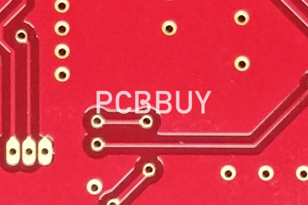
A via is a plated-through hole in a PCB that you can use to route a trace from your board's surface layer to the inner and other layers. It is essential to realize that you can drill PCB vias mechanically, and you can plate them to create electrical connections.
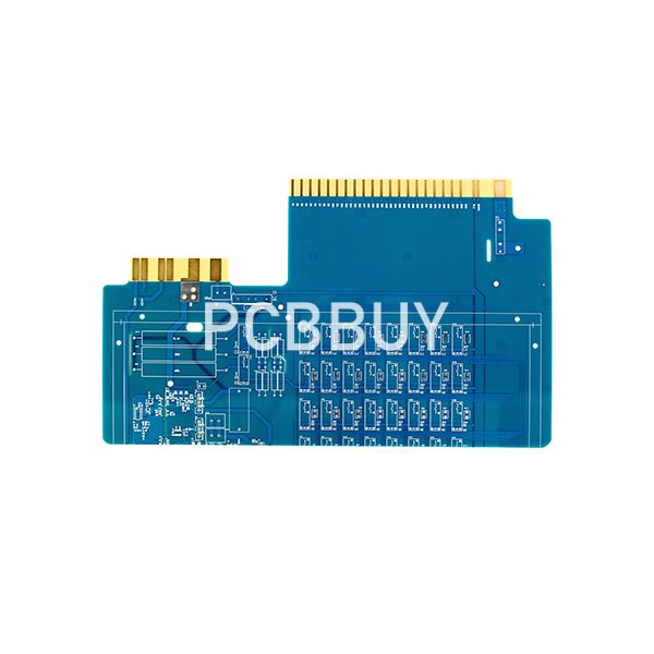
Vias are vital in multi-layered PCB boards, which are challenging to design and produce. They create routes for the sufficient flow of electrical and thermal current between the board's different layers. This article presents all the basics- not forgetting the via-production process, the primary types, and PCB design tips for vias.

What Are the Types of PCB Vias?
There are two primary categories of vias, depending on where they are in the PCB layers — the blind hole and the buried hole.
In a blind hole, the hole penetrates the top or bottom layer of the board but stops before any of the internal layers. Blind holes are named as such because you cannot see through them when you hold a board up to the light. The process involved with blind-hole creation can be difficult because you must know when to stop drilling into the board. As such, many PCB manufacturers avoid hole plating of this type.
Another type of via is the buried hole, which might appear through one or more internal layers. Since the buried hole is sandwiched between layers, it cannot be seen by the naked eye. For a multi-layer board to have a blind layer, the hole plating on the internal layer must be completed early on during PCB assembly, before the top and bottom layers are applied to the board.
1. Through-Hole
The most obvious type of via is the plating through-hole, which penetrates all the layers in a multi-layer board. Through-holes are typically larger than blind holes and buried holes and are also a lot easier to identify with the naked eye. When you hold a board up before the light, the light will pierce right through a plating through-hole. Through-holes are also easier to make because you can simply drill right through all the layers, unlike with blind holes, where you have to be careful how deep you make the hole.
Through-hole technology has been around since the mid-20th century when it replaced point-to-point construction. Through-holes were most common between the 1950s and 1980s when nearly all the features found on a printed circuit board were attached to a through-hole.
In the early days of through-hole technology, PCBs had their tracks printed only on the top side. As technology advanced, the printing appeared on both sides. Eventually, multi-layers boards came into use. At this point, through-holes were updated to plated through-holes to enable contacts between conductive layers. Today, plated through-holes are used to connect the different layers in a PCB. Through-holes are usually used to facilitate components with wire leads. Axial-leaded components are placed through these holes and used to connect across short spaces.
2. Via-in-Pad
One of today’s more popular designs for printed circuit boards involves the application of vias on ball grid array (BGA) pads, alternately known as via-in-pad. In the via-in-pad design, the vias are placed on the BGA pads of the PCB. The design has become popular because it makes it possible for manufacturers to minimize the amount of space required for vias.
The via-in-pad design is especially convenient for routing because the holes connect straight to the layer that underlies the component, making it possible to route signals without the risk of going outside the perimeter of the device’s footprint.
In a standard via layout, solder mask can be applied to stop the flow of solder into the via. With the via-in-pad design, you cannot leave the barrel free of filling because air could get trapped, causing out-gassing while the PCB is in production. Therefore, the vias need to be filled when placed on BGA pads. For the design to work, you must also have a flat planar surface, as this will make it possible to connect fine-pitch BGAs with little, if any, complications.
3. Microvias
In PCB design, vias that are under 150 microns are known as microvias, which are used on many high density interconnect (HDI) boards. Designers prefer microvias because of the small size of the hole, which consumes far less space on the board than the holes that require more drilling. In a microvia, the layers are connected to one another with copper plating.
Microvias are created in the shape of cones, which makes it easy for the via sides to be copper plated. A microvia can go through two adjacent layers but not any further. If a board design requires a via through multiple layers, multiple microvias would need to be stacked accordingly.
From a manufacturing standpoint, creating stacked microvias can be a costly and time-consuming process. On boards that require one microvia over another, the most common design will feature two microvias. As far as stacking is concerned, the ultimate limit is four microvias. However, four microvias are rarely applied in PCB manufacturing because of the high costs.
An alternative option to the stacked microvia is the staggered microvia, which is set up like a staircase where a second or third microvia is placed a step forward below the one above. As with stacked microvias, staggered microvias can be difficult and costly to produce on a multi-layer PCB.
A microvia that connects two inner layers in a PCB is known as a buried microvia. For a buried microvia to be included in a PCB design, the layers that contain the holes must first be drilled before the outer layers are applied. With a buried microvia, you can connect two inner layers on a printed circuit board. The drilling can be accomplished with a mechanical tool or, alternately, with a laser.
When you place a microvia on a PCB, it is crucial to pay attention to the aspect ratio of the hole size, otherwise, it might be impossible to plate the board properly.
What Is the Importance of Via of PCB?
If you have a simple circuit board, you may not need vias. But you need vias when you are dealing with a multi-layered board, as mentioned earlier.
Vias will help you to establish an excellent component density in multi-layered boards.
Besides, they also raise trace density in multi-layered boards as you can run them over and beneath each other in different directions. Vias allow the various traces to link with each other. In this case, they act as vertical connection factors.
If you fail to incorporate vias into a multi-layered PCB routing process, you will end up placing your components densely. Lastly, you need vias to facilitate the transmission of signals and power between layers. If you do not want to use vias, you should route your PCB components on a single plane. Remember, surface mounted parts in a multi-layered PCB make it impossible to route components on a single plane.
Industry Category


