What is a Solder Bridge and How Can It Be Removed from PCB?
By:PCBBUY 12/08/2021 09:38

Solder bridging is just one of the many soldering issues that can occur on your PCB during its manufacturing journey. And as its name suggests, it takes place when two or more pads become connected through an excessive application of solder, creating a bridge.
In this passage, if you are searching for the definition of solder bridge and the methods to prevent it, please check and read the content below for more information.
Wanna know PCB knowledge? Check and read for more.
What is the basic information of Solder Bridge in PCB?
To have a perfect understanding of what bridge soldering is, you have to know what soldering is. Soldering is a way of bringing small pieces together on the surface of a circuit board. It connects electrical components on a PCB. Soldering is an important aspect of PCB manufacturing.
During soldering, materials such as soldering iron, soldering paste, and solder flux are used. The soldering process is simple and straightforward. However, mistakes occur. Therefore, bridge soldering is one of these mistakes.
Bridge soldering occurs when two or more component pads connect due to excessive use of solder. Normally, these pads are not meant to connect electrically on PCBs. This situation causes electrical shortages that can result in different kinds of havoc.
What are the causes of Solder Bridge in PCB?
While there is no way to guarantee you never see solder bridges on your circuit boards, there are a few key things you can do in your design and preparation to greatly reduce your solder bridging risk.
Use the correct lead lengths for through-hole parts
Through-hole components with leads that are too long can cause solder bridges. The correct lead lengths for your application will depend on the size and thickness of your PCB, the size and mass of the component, and the type of soldering you plan to employ (wave, selective, etc).
Use the correct hole size and pad diameter for through-hole parts
Many solder bridges are the result of holes and/or surface pads that are too large. An annular ring pad that is too large decreases the distance between the solderable surfaces of two adjacent pins. This decreased distance, especially in a wave solder operation, greatly increases the risk of a solder bridge. So follow datasheets to correctly size both the plated through hole and the pad.
Design to the highest producibility level possible
Designing for producibility applies to both surface-mount and through-hole components and relates to the ease of producibility given the dimensions and spacings of your land patterns for your parts.
The IPC (Association Connecting Electronics Industries) publishes industry standards for PCB design and assembly, and they have defined Level A as the preferred level for general producibility. In some designs very small spacings are unavoidable, but in many designs, they are very avoidable. The best practice here is to avoid using unnecessarily small parts or tight spacing.
How to prevent Solder Bridge in PCB?
Worried about how to prevent solder bridging? While PCB designers have no control over the assembly process, there are some areas that you can work on to reduce the occurrence of solder bridging. The first thing is to ensure that the stencil thickness is not causing excessive solder paste to be deposited on the pads. If it is, you’ll need to produce a thinner stencil.
Ensure that component pads are designed with the right dimension. Pads shouldn’t be too wide or too narrow. If you’re in doubt, refer to the IPC standards on the dimension for optimum solderability. It also helps if you’re designing with component libraries that are in compliance with IPC standards.
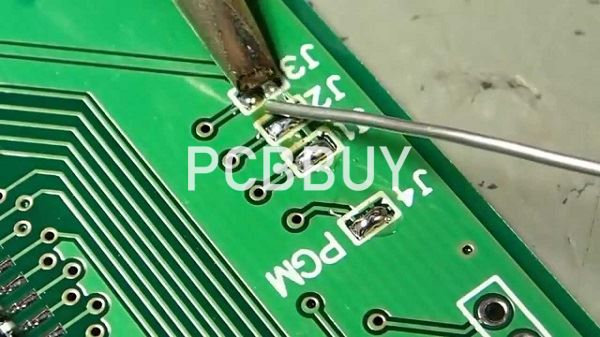
Even with all the precautionary measures, solder bridging may still occur. To fix that, you’ll need to use a narrow tip solder iron, wet it with a solder paste, and heat up the solder bridge. Gently drag out the melted solder out of the pads. Then, test with a multimeter to ensure that the pads are no longer shorted.
How to fix Solder Bridge of PCB?
There are several reasons why solder bridging occurs. This includes incorrect use of solder masks, excessive solder, incorrect soldering technique. This defect can be avoided at times. However, there are times it happens. It is, therefore, important to learn how to fix this problem. To fix a solder bridge, you need a solder flask, solder wick, and temperature adjustable soldering iron. Follow these steps to fix a solder bridge.
Monitor the temperature
Usually, you want a large tip to transfer sufficient heat into the solder wick. You need to monitor the temperature. Ensure the temperature is higher than the soldering temperature. This will compensate for the solder wick absorbing some heat from the joint.
For instance, if you solder at 270°C, you would have to increase the temperature to 300°C when utilizing the solder wick.
Surface tension
Surface tension refers to the possibility of fluid surfaces to shrink into the smallest area possible. The type of skills you have got and how effective your flux is might help you to wick the bridge away without needing a solder wick. You can utilize surface tension.
Surface tension helps to remove the solder from the bridge. You can fix a solder bridge without utilizing a solder wick. You just need to clean the top of the soldering iron before you try again. However, you need to be careful, heating the pin or pad severely with this approach can damage the integrated circuit or PCB pad.
Industry Category


