Annular ring in PCB
By:PCBBUY 06/29/2021 16:55

Do you know what is annular ring in PCB?Since annular ring is a very important factor during the PCB manufacturing process, it is necessary for us to get into the knowledge of annular ring. In this passage, we will lead you to learn every detail of annular ring, please follow us and read the content we prepare for you below.

What is annular ring?
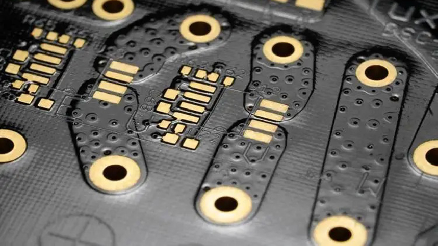
When you drill a hole into a copper PCB pad, the resulting copper surrounding the hole is what we know as annular rings. It essentially acts as the wall of the drilled via. Your annular ring size will depend on the size of the via and the size of the copper pad’s size.
But what is the purpose of the annular rings? As you may or may not know, PCBs are multi-layered. Your circuit board traces will need to connect to various layers of your PCB. They usually achieve this by reaching a pad which routes them through to another layer by a via.
The annular ring surrounding the via facilitates the connection between the trace and the via. What this means is the thicker the annular ring, the stronger the connection. But how thick should the annular rings be, and how do you calculate it?
How to calculate annular ring?
To find an annular ring’s width, you need to use this formula: (pad diameter – via diameter) ÷ 2.
If the diameter of the pad is 25 mils (0.50mm) and the hole/via is 15 mils (0.38mm) then your equation will look like this:
(25 - 15) ÷ 2 = 5 mils
(0.50 – 0.38) ÷ 2 = 0.06mm.
Let us look at further real-world examples. That will include the annular ring's width for standard vias, micro via, and component holes.
Standard Via
Generally, a standard via will feature a hole with a diameter of 0.20mm (7.87 mils). On a 0.40mm (15.74 mils) pad, your final equations will look like this:
(0.40mm – 0.20mm) ÷ 2 = 0.10mm
(15.74 mils – 7.87 mils) ÷ 2 = 3.93 mils
Microvia
Micro vias are typically smaller than your standard holes. They will have a hole diameter of 0.10mm (3.93 mils). On a pad with a diameter of 0.30mm(11.82mm), your equation will look like this:
(0.30mm – 0.10mm) ÷ 2 = 0.10mm
(11.82 mils – 3.93 mils) ÷ 2 = 3.93 mils
Component Hole
As we discussed earlier, component holes tend to be larger than average vias. On a pad with a 1.20mm (47.24 mils) diameter and a 0.80mm (31.50 mils) hole, your equation will look like this:
(1.20mm – 0.80mm) ÷ 2 = 0.20mm
(47.24 mils – 31.50 mils) ÷ 2 = 7,87 mils
Why is the width of annular ring important?
As discussed earlier in the guide, the annular ring connects to the traces and the various layers of the PCB. Thus, it should be sizeable enough to support a reliant connection. The thicker the annular ring, the stronger the connection around the via will be. If the annular ring is not thick enough, it may cause connection issues or breaks.

You may have heard the term “teardrop annular ring” before. Teardrop pads feature additional copper near the junction of the annular ring that connects to the PCB traces. They assist in creating a more secure connection that may be more resistant to stress.
The idea here is simple. The more copper around the via, the thicker the annular ring is, and the stronger the signal it can carry to and from the traces.
How to position via in annular ring?
Not only do your annular rings have to be ample in size, but you need to position the hole (via) correctly. If you have positioned the hole too close to the pad’s boundaries, it could cause a tangency. Additionally, a tangency may also occur if the annular rings are too thin.
Nevertheless, when you drill your hole, you want to drill through the center of the copper pad. That will give you the most structurally efficient annular rings. Drilling too close to the pad’s edges will give you a compromised or bad via, which will effectively end in a tangency.
Drill too far from the middle of the pad could end up in a breakout. This is when the drill offsets the hole and breaks the pad’s boundaries’ continuity, resulting in a structurally insufficient annular ring.
The annular rings structure is largely dependent on where you drill your hole and place it via. It would help if you avoided both a breakout and tangency when you assemble your PCB. Nonetheless, this is how vias and annular rings are related.
Industry Category


