Backplane in PCB
By:PCBBUY 07/29/2021 17:15

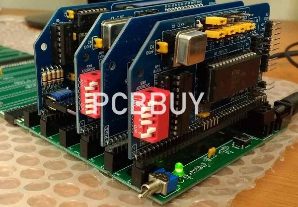
The term Backplane PCB generally refers to larger format printed circuit boards that are used as backbones for connecting several PCBs together to ultimately form a computer bus. they serve as a connection center between active duty PCBs. Backplane PCBs often incorporate a wide variety of features including blind / buried vias, high-speed / high-signal integrity materials, back drilling, and controlled impedance.
In this passage, we will provide all the details information of backplane in PCB. If you are curious about it, please check and read the content to learn professional knowledge.
What is the definition of backplane in PCB?
Backplane PCB, also called motherboard, is a type of baseboard responsible for carrying function boards including daughter boards or line cards. The major task of backplane board is to carry daughter boards and to distribute power to function boards so that electrical connection and signal transmission can be achieved. Therefore, the system function can be acquired through the cooperation between backplane and its daughter boards.
As IC (Integrated Circuit) component features increasingly higher integrity and I/O count keeps rising, together with rapid progress that is made in electronic assembly, high frequency of signal transmission and the development of high-speed digitalization, the functions of backplane board gradually cover function board carrying, signal transmission and power distribution. In order to implement those functions, backplane boards have to reach higher requirement in terms of layer count (20 to 60 layers), board thickness (4mm to 12mm), via count (30,000 to 100,000), reliability, frequency and signal transmission quality.
Accordingly, to obtain such high requirement in performance, backplane PCB fabrication have to be confronted with rigorous challenge on board thickness, board size, layer count, alignment control, back drilling depth and stub. In other words, all the mentioned aspects are definitely key issues as far as backplane fabrication is concerned. This article aims to display the key difficulties met in backplane PCB fabrication process and discuss some handy tips based on PCBCart’s more than ten years’ manufacturing experience.

What are the features and benefits of backplane in PCB?
· Ease of assembly as circuit 1 and 1,000 are built with the same tooling guaranteeing reproducibility
· Larger sized backplanes eliminates “jumper” cabling within a chassis improving reliability, lowers assembly cost and creates stronger signal integrity
· High performance materials for high speed digital applications
· Wide range of material selections to suit the design from power to high-speed (56gb) applications
· Copper weight variability to carry high speed signal or power within one design
· Precision back-drilling for high-speed signal integrity
What are the difficulties of backplane PCB manufacturing?
Alignment Control
Alignment control is the foremost manufacturing difficulty as far as ultra-multi-layer PCB fabrication is concerned since bad alignment control will possibly lead to shorts.
![]()
Alignment control is affected by numerous procedures and elements among which layer stack-up most matters. Multi-layer PCBs usually have three types of compositions: mass-lam, pin-lam and thermocouple heating.
Tips:
· The optimal composition method lies in pin-lam since it won’t arouse shock effect on core board.
· When pin-lam can’t be applied due to some limitations, copper-iron rivets plus short dowels will be a good selection.
· As pin-lam stack-up is used, which category of pins is used is extremely significant. For example, we find that four pins are used to perform better than eight circular pins, compatible with the requirement on alignment control.
Drilling Technology
Due to high thickness of backplane board, drilling is possibly too short to reach the board. Too long drilling tool, however, tend to suffer from breaking during drilling process. In addition, too much dust may block the hole and burr may be caused, dramatically reducing backplane PCB performance.
Tips:
· CCD method should be applied in drilling backplane board and CCD marker depends on the hole drilled through X-ray drilling.
· Drilling depth can be accurately determined through the application of depth control in a conductive way.

Electroplating Capability
Due to high thickness of backplane board, the aspect ratio will be high as well. To make sure sufficient copper at hole, if the electroplating cannot be deep enough, sufficient copper will be inside hole while too much copper will be left at hole mouth, affecting aperture, leading via aperture and copper thickness at hole wall to be incompatible.
Tips:
· Pulse plating solution should be compared with DC plating solution in terms of plating capability, reliability and solution stability.
· New DC plating solution should be used, such as EP.
ICD Analysis
ICD tends to be occurred during the process of high-frequency material fabrication, causing dramatic quality risk on electrical connection and long-term reliability. The cause for ICD and its solution should be summarized so that such issues can be avoided in the process of backplane PCB manufacturing. The cause for ICD issue lies in the resin gel residue left on inner copper layer and insufficient cleaning is carried out.
Tips:
· Board material aging extent should be analyzed to stop resin due to insufficient aging being left on inner copper layers.
· Drilling parameter control should be optimized to certify that gel residue has been eliminated.
Backdrilling Stub
As far as high-speed signal transmission is concerned, stub will lead signal to be distorted or even signal transmission failure. Therefore, the negative effect caused by stub on high-speed signal transmission should be clarified. Up to now, it can be summarized that when the length of stub is less than 0.25mm, its effect on signal is quite low and can be ignored. As a result, stub length should be controlled within 0.25mm.
Tips:
Stub length should be controlled within 0.25mm to minimize its effect on signal transmission quality.
Industry Category


