Blind via in PCB
By:PCBBUY 06/10/2021 17:49

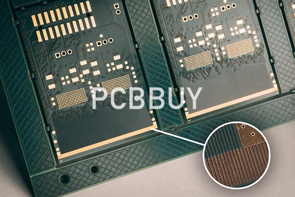
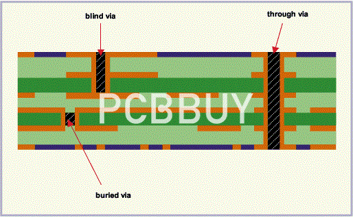
Blind via links the surface layer of PCB and the internal layers. Another point to note is that blind vias do not pass through the whole board. The surface layer is usually one and is either the upper or lower part of the board. Contrary, the internal layers can be more than one. That is why you can only see blind vias on one part of aboard.
The need to link components to the two sides of these complex printed circuit boards should be among your priorities when designing a PCB. Basically, you require blind and buried vias to connect components to various sides of your PCB. The article takes a deep dive into the different vias available, the uses, advantages, and disadvantages.
What are the features of PCB with blind via?
In summary, following are the clear-cut features that you will observe in PCBs with Blind vias:
1. They will have more holes than a traditional PCB. If the PCB is four-layered, the extra holes will only join two layers.
2. They will have higher pad density and wiring than traditional PCBs.
3. There will be reduced trace space and width.
4. During the fabrication process, they follow a slightly complex build-up process.
5. They are an inexpensive solution.
Amazingly, there is another very beneficial type of vias – the buried vias. In the next chapter, we have discussed it in detail and have compared it with blind vias.

What are the applications of blind via PCB?
This part will take a closer look at the two primary uses of blind vias in circuit boards. It is essential to realize that you can minimize your circuit board layers by expanding the ball-grid getaway channel. You can achieve that by creating blind vias.
Are you experiencing difficulties when penetrating through-hole vias for designing and trace breakout of BGA? If so, try increasing the getaway channels on the internal and lower layers with blind vias. Alternatively, you can use blind vias to reduce your circuit board aspect ratio.
Mostly, circuit board BGA components come with various pitches. For example, a 4.00mm radius board contains 0.8mm and 1.27mm pitch BGAs. Remember, the smallest size via hole is determined by both the drill and board aspect ratios.
How to make blind via PCB?
PCBs with blind vias follow the standard procedure of making multilayer PCBs, only till the drilling stage. They offer extra holes that make a connection between only two layers if the PCB is four-layered. Before starting the PCB designing procedure, decide what build-up are you going to use and check with the PCB manufacturer.
If you are someone who considers adding vias ‘on the go’; you may have to face dire consequences. Your PCB space will run out and eventually; you may have to discard the board and re-design everything. Furthermore, it will waste your time, energy and money. So, to save you from these consequences, we will describe in detail how to add blind vias to your PCB.
Before going forward, we will mention the basic rules that all blind vias must follow:
·The must begin from either the bottom or top layer of the printed circuit board.
·The must occupy an even number of layers, i.e., 2, 4, 6 and so on.
·They should never go through the whole printed circuit board.
·They can never begin or end at the center or core of the PCB substrate.
Recall that blind via in the printed circuit board, with multiple layers, makes a connection between the surface layer and internal layers. However, due to certain limitations, it is a complicated task to drill a blind according to the modeled depth. For good plating or metallization quality, via sizes should be correctly selected

The hole depth to hole diameter, H/d value, should not be greater than 1, and 0.8 is ideal value. Thus, the deep vias should have large diameters. Moreover, huge vias also mean that the dielectric gap between PCB layers is also huge.
To properly make the blind vias, you would need to first bore the vias in the center cores. Then, make the vias go to the surface layers of PCB. In the end, prepreg assists in stacking together the PCB layers.
In conclusion, we will say that you must compare your circuit requirements with the processing abilities of PCB manufacturer. Additionally, PCB manufacturers have often mentioned rules that must be followed to make PCB producible. Thus, it is good practice to learn about the design rules of blind vias, as provided by the PCB manufacturer.
Industry Category


