Copper clad PCB
By:PCBBUY 07/16/2021 17:30

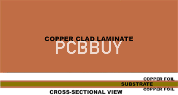
The PCB substrate in PCB manufacturing - Copper clad laminate (CCL), which is the most widely and important used to fabricate the PCB. The copper clad laminate is a type of material that soaks in resin with the electronic glass fiber or other reinforcing material to make with copper clad on the sides. And it’s widely applied in television, radio, computer, mobile communications and other electronic products.
In this passage we are talking about the copper clad and if you are curious about it, please check the content we prepare for you below.

What are the copper clad lamination types?
With the development of small, light, thin, multi-functional and high-density electronic products, the integration and assembly density of components on the boards are more and more higher, as well as power dissipation is more and more larger, so the heat dissipation has a great demand on PCB substrates. There will be overheated for the components on the board if the substrates have a poor dissipation, which will lead to the unreliability of whole machine. So the PCB substrate comes into being.
There are a lot of kinds of copper clad laminate based on different standard of classification.
1. Classified by reinforcing material:
· Paper base CCL ( such as XPC)
· Glass fiber cloth base CCL (such as FR-4, FR-5)
· Compound CCL ( such as CEM-1, CEM-3)
· Special material base CCL (such as metal-base CCL, ceramic-base CCL and so on)
2. Classified by applied insulation resin:
· Phenolic resin CCL (such as XPC, XXXPC, FR-1, FR-2 and so on)
· Epoxy resin CCL (FR-3)
· Polyester resin CCL
3. Classified by performance:
· General performance CCL
· CCL with high heat resistance
· CCL with low dielectric constant
· CCL with low CTE (Coefficient of Thermal Expansion)
4. Classified by mechanical rigidity:
· Rigid CCL
· Flexible CCL
What are the materials of copper clad lamination?
Copper foil: copper foil is a cathodic electrolytic material that deposited on a thin and continuous layer of metal foil on the base of PCB. And it’s easy ti bond to an insulating layer making a printed protective layer and create a board pattern with corrosion.
Prepreg: A prepreg (from pre-impregnated) is fibreglass impregnated with resin. The resin is pre-dried, but not hardened, so that it will flow, stick and completely immerse as heating. So prepregs are fibreglass strengthened by an adhesive layer (similar to FR4 material). as well as it’s known as the types of fibreglass.
Different manufacturers have different thickness in the types of prepreg, what’s more, there are the versions "SR" Standard Resin, "MR" Medium Resin "and" HR "High Resin based on the resin content. The best possible material is used depending on the desired final thickness, layer structure or impedance. The mentioned thicknesses are thus to be considered only as examples.
What are the standards of copper clad lamination?
ASTM D1867 defines the standard specification for copper clad laminates that manufacturers use for making printed circuit boards. Covering twelve grades of copper clad laminates, ASTM D1867 requires the laminates to meet peel strength at elevated temperatures, crosswise and lengthwise flexural strength, flammability ratings, volume resistivity, water absorption, dielectric breakdown, dissipation factor, and permittivity. The laminates must further conform to tests for blistering, warp, and twist.
Manufacturers of copper clad laminates follow the IPC-4101C as their manufacturing standard, and the IPC-IM 650 for testing the copper clad laminates they fabricate.
What are the advantages of copper clad lamination?
Using copper clad laminates for PCBs allows designers take advantage of constant distance between the copper foils acting as power and ground planes. When distributing power to a system, this arrangement reduces the modal resonances by lowering the inductance between the two planes. This not only reduces the impedance of the system, but also decreases the amount of filter capacitors necessary.
Industry Category


