What is function of solder mask in manufacturing process?
By:PCBBUY 10/08/2021 09:57

Solder mask is a thin layer of polymer that is put on a circuit board to protect the copper from oxidation and shorts during operation. It also protects the PCB from environmental influences such as dust and several other contaminants that may lead to shorts in the long run.
In this passage, we will focus on the function of solder mask in manufacturing process. If you are interested in function of solder mask, please check and read the content for more information.

How to apply solder mask on PCB?
Solder mask is made up of a polymer-layer that coating over the metal traces on a board. There are a number of different types of mask material, the best option for your PCB according to your application and cost. Printing a liquid epoxy over the board with a silkscreen is the most fundamental solder mask option, which is like airbrushing face paint on with a stencil.
Solder mask comes in different media depending upon the demands of the application. The lowest-cost solder mask is epoxy liquid that is silkscreened through the pattern onto the PCB. Other types are the liquid photoimageable solder mask (LPSM) inks and dry film photoimageable solder mask (DFSM). LPSM can be silkscreened or sprayed on the PCB, exposed to the pattern and developed to provide openings in the pattern for parts to be soldered to the copper pads. DFSM is vacuum laminated on the PCB then exposed and developed. All three processes go through a thermal cure of some type after the pattern is defined.
What are the 4 types of solder mask?
Top- and Bottom-side Masks
A topside solder mask allows the electronic engineer to identify the openings in the green solder mask layer already added to the PCB by one of the epoxy, ink or film techniques. Component pins can then be soldered onto the board using those identified places.
Epoxy Liquid
Silkscreened onto the PCB pattern, epoxy liquid is the lowest cost type of solder mask. Epoxy is a thermosetting polymer that has many applications. Silkscreening is a printing technique that uses a woven mesh to support ink-blocking stencils or patterns.
Liquid Ink Photoimageable
Liquid photoimageable solder mask is delivered as an ink formulation. The ink can be silkscreened or sprayed onto the PCB, then exposed to the pattern and developed. One type of process commonly used with liquid ink formulations is hot air surface leveling (HASL).
Dry Film Photoimageable
Dry film photoimageable solder mask is applied using vacuum lamination, then exposed and developed. After developing, openings are created in the pattern and parts can be soldered to the copper pads. Copper is layered onto the board inside the holes and on the trace areas using electrochemical processing.

What is the function of PCB solder mask?
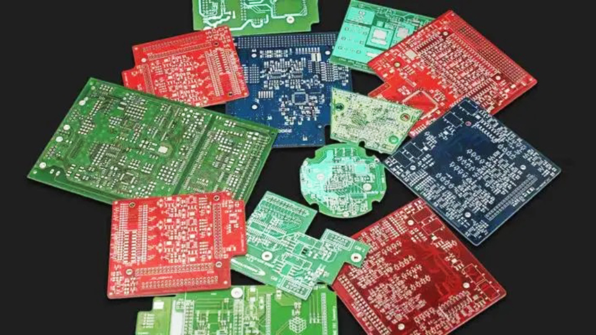
Solder mask or solder stop mask or solder resist is a thin lacquer-like layer of polymer that is usually applied to the copper traces of a printed circuit board (PCB) for protection against oxidation and to prevent solder bridges from forming between closely spaced solder pads. A solder bridge is an unintended electrical connection between two conductors by means of a small blob of solder.
PCBs use solder masks to prevent this from happening. Solder mask is not always used for hand soldered assemblies, but is essential for mass-produced boards that are soldered automatically using reflow or solder bath techniques. Once applied, openings must be made in the solder mask wherever components are soldered, which is accomplished usingphotolithography.Solder mask is traditionally green but is now available in many colors.
Solder mask comes in different media depending upon the demands of the application. The lowest-cost solder mask is epoxy liquid that is silkscreened through the pattern onto the PCB. Other types are the liquid photoimageable solder mask (LPSM) inks and dry film photoimageable solder mask (DFSM).
LPSM can be silkscreened or sprayed on the PCB, exposed to the pattern and developed to provide openings in the pattern for parts to be soldered to the copper pads. DFSM is vacuum laminated on the PCB then exposed and developed. All three processes go through a thermal cure of some type after the pattern is defined.
In electronic design automation, the solder mask is treated as a layer of the printed circuit board, and is described as a Gerber file like any other layer, such as the copper and silkscreen layers.

What are the tips of solder mask design?
As a matter of fact, solder mask is optional no matter what type of PCB design software you prefer to use. Solder mask can be easily designed through completing filling some parameters. Some software even can provide an automated solder mask.
Prior to real design, it's of much necessity to contact with contracted PCB manufacturer to be correctly aware of their capability in terms of solder mask thickness and minimized spacing between copper pads neither of which is cure-all for every piece of board.
Circuit board will fail due to silly issues concerning solder mask such as insufficient solder mask opening, excessive openings, mismatching between number of openings and that of copper pads in circuit plane. Those issues possibly derive from carelessness or design file modification but do take much time for confirmation. And some even arouse catastrophes. Therefore, your design files are dramatically worth your careful examinations.
Industry Category


