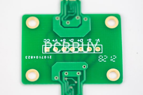
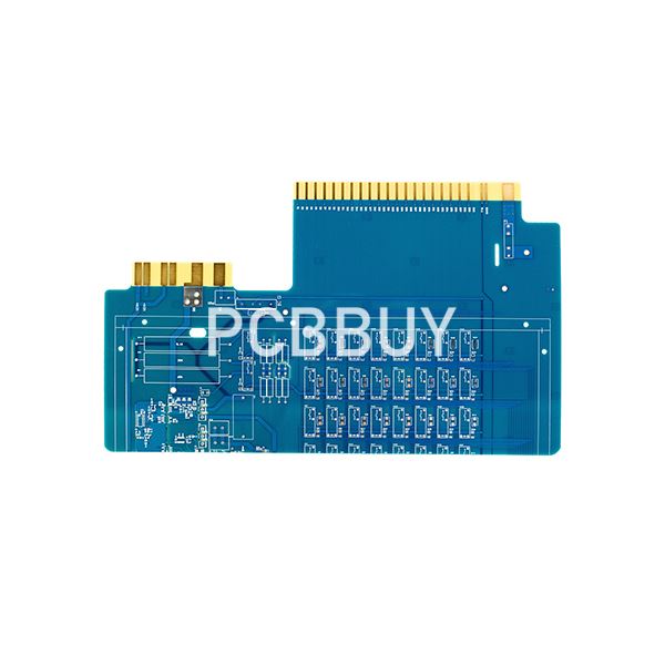
PCB gold finger
By:PCBBUY 05/21/2021 17:25

Gold Fingers are the gold plated narrow connectors found on the edge of printed circuit boards to enable connections between multiple boards. And they aim at connecting the secondary circuit board to the motherboard of a computer. Because the alloy has a great conductivity, gold is used in the connecting points along the board. They are made from flesh gold, the hardest form of gold available and work for a long time with superior conductivity. The thickness of gold fingers usually ranges from 3 to 50 microns.
Gold is chosen for these fingers as it has the highest corrosion resistance and electrical conductivity after Copper and Silver. Sometimes, Gold is combined with Cobalt and Nickel to increase the resistance of the fingers for wear and tear. PCBs are connected/disconnected from each other multiple times. So these connection points (fingers) need to be able to handle some wear and tear.
In this passage, we will provide the knowledge of the gold finger in PCB manufacturing process. Please check the content below for more.
What is gold finger?
Gold fingers are the gold-plated columns that you see along the connecting edges of printed circuit boards (PCBs). The purpose of gold fingers is to connect a secondary PCB to the motherboard of a computer. PCB gold fingers are also used in various other devices that communicate via digital signals, such as smartphones and smartwatches. Gold is used for the connecting points along a PCB because of the alloy’s superior conductivity.
There are two types of gold applicable to the PCB gold finger plating process:
Electroless Nickel Immersion Gold (ENIG): This gold is more cost-effective and easier to solder than electroplated gold, but its soft, thin (typically 2-5u” composition renders ENIG unsuitable for the abrasive effects of circuit board insertion and removal.
Electroplated Hard gold: This gold is solid (hard) and thick (typically 30u”), thus more ideal for the abrasive effects of constant PCB usage.
Gold fingers make it possible for different circuit boards to communicate with one another. From the power source to the device or equipment, signals must pass between several contacts for a given command to be enacted.
Once you press a command, the signal will pass between one or more circuit boards before it is read. For example, if you press a remote command on a mobile device, the signal will be sent from the PCB-enabled device in your hand to the near or distant machine, which in turn receives the signal with its own circuit board.
The process involved in the plating of gold fingers involves a number of meticulous steps. This ensures each circuit board rolling off the production line is properly equipped to conduct signals free of error. The standards involved in the plating process also helps to ensure a perfect fit between the gold fingers on each circuit board with the corresponding slots on a given motherboard.
To ensure that all of these fingers and slots fit hand-in-glove, each PCB must pass a series of inspections and defect tests. If the gold plating on a circuit board lacks smoothness or does not adequately adhere to the surface, the results will not be sufficient for commercial release.
For PCB gold fingers to come together, the plating process must be carried out in steps where the surrounding details of the board are completed first. When the time comes to plate the fingers, nickel is applied over the copper. Then, the surface finish is applied last. Once everything has set, the board is inspected under a magnifying lens and subjected to adhesion tests.
How are gold fingers applied?
Gold fingers can be used for many various things. And they use depending on the designer’s purpose. There are some common applications of gold fingers as the follows:
1. Provide an interconnection point for transferring network data;
2. Connect external components to the PCB prototype;
3. A place for attaching specialized adapters or daughter boards;
4. Serve as an audio adapter
What are the specifications of gold finger?
There are some standards you need to follow for the gold fingers so that it can work correctly during the plating process of gold finger. As well as the PCB design need to take into account the areas where is necessary to proper finger length and alignment. The rules can be used for the gold finger design as the follows no matter what the size or the purpose of the circuit board:
1. Plated through hole should far away from the gold fingers;
2. There should be kept at a distance between gold fingers and solder mask or screen printing;
3. Gold fingers should always keep the opposite direction from the middle of the board.
Industry Category


