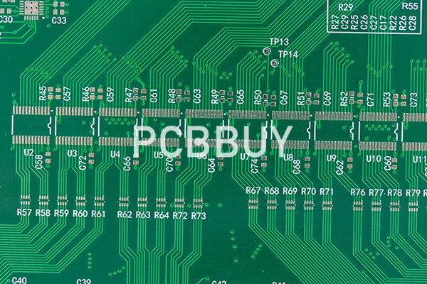
PCB grounding
By:PCBBUY 06/01/2021 18:34

A ground is a conducting body that acts as an arbitrary node of potential voltage and a common return for electric current. It is a point of zero reference or zero volts. The ground is the reference against which you base the signal.
There are also special considerations when working in a mixed-signal analog and digital environment. Grounding can help to minimize noise when working with signals that have a wide dynamic range.

What are types of grounding?
There are various types of nodes that get called grounds including floating grounds, virtual grounds and earth grounds.
Floating grounds: These nodes are reference points in an isolated system and are not physically connected to the earth.
Virtual grounds: These nodes can be found in a negative feedback circuit at the inverting terminal of an operational amplifier. When the non-inverting input is at zero volts, the feedback will make the inverting terminal match it in a stable circuit. The value is not a stable return for other circuits and is only held by feedback.
AC grounds: These nodes have low-impedance DC values. This DC voltage is stable even when exposed to small disturbances. Because of its DC value, this node can’t be used as a proper ground, but because it is stable, it can be used as a reference point.
Earth grounds: In a large electrical system, the earth’s ground is literally a connection to the ground. Every house, for example, has a copper pole that is stuck in the earth to deplete surplus currents.
Chassis grounds: The electronics in a PCB cannot connect to the physical ground, but a chassis ground serves the same purpose. This ground is the connection of a safety wire from the AC mains to the product’s case or chassis.
Because an earth ground and chassis ground serve the same function, these terms are often used interchangeably along with the term safety ground.
When it comes to grounding a PCB, there is no one-size-fits-all approach. To determine the best way to ground a system, you need to understand the way the currents within it flow. There are, however, various methods to choose from and some tips for best grounding practices that apply across the majority of systems. To determine the approach that works for your board, you’ll need to ensure you understand the board’s design and may need to try several techniques.

What are PCB grounding techniques?
There are various techniques that one can use for grounding a PCB. The following are some of the most common approaches used today.
1. Ground Plane
One common technique is to use a ground plane, which is a large piece of copper on a PCB. Typically, PCB manufacturers will cover all of the areas that don’t have a component or trace on them with the copper ground plane.
In a two-layer board, the standard PCB ground plane rules indicate that the ground plane should be placed on the board’s bottom layer, while the components and signal traces are on the top layer.
It is best to avoid creating a ring of conductive material formed by the ground plane, as this makes the ground plane more susceptible to electromagnetic interference (EMI). This conductive ring acts as an inductor, and an external magnetic field may cause an electric current called a ground loop. You may end up with a conductive ring if placing the ground plane over the whole bottom layer and then removing the parts that have electronic components.
The ground plane is also often on both sides of the board. In some cases, the plane on the component side is kept at the supply voltage, and the plane on the other side of the board is grounded. The ground plane is connected to the ground pins of the components and connectors to keep the ground voltage at the same level through the whole PCB.
2. Ground Plane Vias
If there are ground planes on both sides of the PCB, they will be connected through vias at many different places on the board. These vias are holes that go through the board and connect the two sides to each other. They allow you to access the ground plane from anywhere you can fit in a via.
Using vias can help you to avoid ground loops. They connect the components directly to the ground points, which connect through low impedance to all of the circuit’s other ground points. They also help to keep the length of return loops short.

Pieces of copper, such as ground planes, may resonate at one-quarter of the wavelength of the frequency of the current which is flowing into it. Putting stitching vias around the ground plane at specific intervals can help to control this.
3. Connector Grounds
All of the connectors in a PCB should be connected to the ground. In connectors, all signal conducts must run in parallel. Because of this, you must separate connectors using ground pins.
Each board will likely need more than one connector pin leading to the ground. Having just one pin may cause issues with impedance mismatch, which can cause oscillations. If the impedance of two connected conductors does not match, the current flowing between them may bounce back and forth. These oscillations can alter the performance of the system and cause it not to work as intended. The contact resistance of each pin of a connector is low but may rise over time. For this reason, it is ideal to use multiple ground pins.
Connectors come in various pitches and can have different numbers of rows of pins. The pins of a connector may also be parallel to the PCB surface or at a right angle to it.
4. Decoupling
PCBs contain one or more integrated circuit chips, which require power to operate. These chips have supply pins to connect them to an external power source. They also have ground pins, which connect them to the ground plane of the PCB. Between the supply and ground pins, there is a decoupling capacitor, which serves to smooth out oscillations in the voltage being supplied to the chip. The opposite end of the decoupling capacitor connects to the ground plane.
One of the main reasons for the use of decoupling capacitors is related to functionality. A decoupling capacitor can act as a charge storage device. When the integrated circuit (IC) requires additional current, the decoupling capacitor can provide it through a low inductance path. Because of this, it is best to place decoupling capacitors close to the IC power pins.
Another primary purpose is to reduce the noise put into the power and ground plane pairs and reduce EMI. Two main issues can cause this noise. One is a decoupling capacitor that does not provide adequate current resulting in the lowering of the voltage at the IC power pin temporarily. The other is an intentional current sent between the power and ground planes using a via with a fast-switching signal.
Industry Category


