Insertion loss in PCB
By:PCBBUY 08/26/2021 10:03

In this passage, we will provide an introduction to the cause and effect of insertion loss which becomes predominant as you push upwards from 3GHz. Energy is lost from a signal as heat in the conductor (the PCB trace and ground planes) resistance and as heat in the dielectric caused by the inherent material properties of the base material itself.
In this passage, follow us and check the content to learn more professional information about insertion loss in PCB. If you are curious about it please read the content below.

Why insertion loss in PCB is important?
At high frequencies signal loss produces signal attenuation and distortion; the signal will be attenuated by conductor resistance and leakage in the laminate material; a signal pulse will be distorted as loss unequally affects each of the signal harmonics. Loss is frequency dependent so each successive harmonic will be increasingly attenuated; the resulting amplitude and changes means the signal at the load will be a distortion of the original.
What are causes of insertion loss in PCB?
If you’ve never worked with RF systems, Wave might sound like an esoteric buzz word. However, the principles involved in Wave design build on those used in lower-frequency designs. Just as is the case with any controlled impedance design, PCB insertion loss arises due to inconsistent impedance throughout an interconnect. This quantity represents the amount of signal that is transmitted at an impedance discontinuity along an interconnect.
· Copper losses: Copper losses occur when the connector's conducting surfaces cause the power to become dissipated. This problem is usually the result of the plating and the material that is used in the PCB.
· Dielectric losses: Dielectric losses occur when the dielectric materials used in the PCB layers causes the power to be dissipated.
· Reflective losses: Reflective losses occur with the connector's voltage standing wave ratio (VSWR) when in transmission lines. It occurs when the power does not become accepted by the load, as it becomes reflected back along the line.
For PCBs using lower speed rates, such as 3Ghz up to 5Ghz, a mismatch in impedance usually results in signal loss. Yet, with the higher speeds of 10Ghz to 30Ghz+, the materials used to create the dielectric constant will be the top issue that could be creating the insertion loss. To deal with these many issues, selecting the appropriate materials for the core, prepreg, and copper foil becomes essential when building the PCB stack-up.

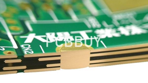
In Wave devices, by far the most prominent source of impedance discontinuities in any impedance controlled interconnect is vias. Layer transitions require some kind of via, whether it is a blind, buried, or through-hole via. Plated through-hole vias or stacked blind/buried vias are typical in traditional multilayer PCB designs. These structures have some parasitic with them, and these parasitic are responsible for producing PCB insertion loss at higher frequencies.
If you look at a time-domain reflectometry trace for an Wave interconnect on a test coupon and calculate the impedance from the interconnect return loss, you’ll likely see a capacitive impedance drop at plated through-hole vias that are used for layer transitions. These impedance discontinuities are undesirable for two primary reasons. First, these capacitive impedance discontinuities at vias cause reflections, leading to the formation of standing waves and strong radiated EMI. Second, this reduces the signal level that reaches the downstream load (i.e., insertion loss).
How to improve insertion loss in PCB?
Dealing with insertion loss can help you design the right high-speed PCB for your application. By understanding the main issues that create this signal loss, you can decide on the types of materials to use for the stack-up, the weave of the glass and resin density, and the thickness of the PCB. To recap on this topic, things to take into consideration for your PCB stack-up include:
· Minimize skin effect and surface roughness of the copper foil by selecting low profile copper, very low-profile ED copper and alternative oxide.
· Select tighter fiberglass weaves for better dielectric constants, or angle and zig-zag the copper traces over looser weaves for signal integrity.
· Choose materials with low dielectric constants and flat frequency responses to handle the multiple signals.
· Use the lowest loss dielectric materials, as well as shorter reaches, to deal with dissipation factors.

What are the differences of insertion loss & connector return loss?
A connector is one of many transmission line elements in a signal path between a transmitter and receiver in a multi-board system. When discussing interconnects, most designers tend to focus on vias as an inductive impedance discontinuity. In other words, a via in an interconnect acts like an inductor at high frequencies and can create some reflection if not designed properly. However, connectors also behave very similar to their own short transmission lines. They also have their own impedance that determines how signals interact with the connector.
As much as we would like connectors to be perfect, the fact remains that they can create some return and insertion loss when placed in an interconnect. The primary mechanism that leads to return loss and insertion loss at a connector is an impedance mismatch caused by surface mount pads on a connector. Through hole connectors also incur some insertion loss as the pins act like inductive/capacitive impedance discontinuities .
Once a signal reaches an SMD connector pad with wider copper, the per length capacitance in this segment of the trace is larger, which then decreases the characteristic impedance of the trace seen at the connector pad. This capacitive impedance discontinuity causes signal reflection and leads to connector return loss and insertion loss.
Industry Category


