Plugged via in PCB
By:PCBBUY 08/02/2021 17:36

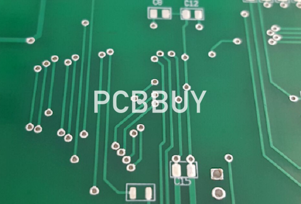
During the PCB manufacturing process, via process is pretty important to affect the quality and performance of the finished boards. Via holes play a role in contributing to electrical connection between layers of PCB. In this passage, we are going to talk about the details of plugged via. Please check and read the content below to learn more information.

What is the introduction of plugged via?
Manufacturing process of solder mask plugging for via holes usually contains via plugging, solder mask application on PCB, prebaking, exposure, developing and curing. The manufacturing process is so long and hard to control that product quality can be seldom guaranteed.
Compared with ordinary solder mask application technology, solder mask plugged via manufacturing shares equivalent procedures except silkscreen printing and post-curing. Thus, the essential point to optimize solder mask plugged via manufacturing process lies in reasonable monitoring and management in terms of silkscreen printing and post-curing.
Silkscreen printing for solder mask plugged via primarily comes in two ways: aluminum sheet and silkscreen. The advantages of aluminum sheet include: small-scale deformation and accurate alignment in silkscreen printing while it features longer procedure and relatively a low manufacturing efficiency. Silkscreen printing refers to the process during which solder mask oil flows into via hole through silkscreen printing.

What are the functions of plugged via?
Solder mask plugging in via holes features the following functions:
a. It is capable of stopping tin on PCB board from going through via holes and being exposed on component surface during wave soldering after components are mounted on circuit board.
b. It is capable of effectively defeating the issue of flux that is usually residual within via holes and further improving products' security.
c. Vacuum negative pressure state is formed on tester after components assembly.
d. It is capable of prohibiting solder paste on the surface flowing into via hole with empty soldering created.
e. It is capable of stopping solder balls from being generated within via holes and further stopping short circuits from being generated by tin ball ejection during reflow soldering.
What are the common issues of plugged via?
Most commonly-seen issues in solder mask plugged via manufacturing process include:
a. Solder mask plugging features bad fullness with copper exposed at via edge.
b. Flatness isn't achieved at via holes with solder mask plugged and solder mask oil is uneven at BGA package.
c. Aperture solder mask oil suffers from bubbles and peel off after the application of HASL (hot air solder levelling) surface finish.
What are the advantages and disadvantages of plugged via?
For PCB designs that require to transfer high amount of heat or current from one side of the board to another, conductive via plugging is a handy solution. It can also be used to dissipate excessive heat generated underneath some components. The metallic nature of the fill will naturally wick heat away from the chip to the other side of the board in many ways like a radiator.
Advantages:
· Heat sink or transfer where other conventional methods are impractical e.g. underneath the chip component.
· Increased current carrying capacity due to higher thermal conductivity (between 3.5 to 15 W/mK) of the conductive material.
Disadvantages:
· High instability of copper pad and copper plating inside the via hole barrel. This occurs due to the difference in CTE (coefficient of thermal expansion) value of conductive material and laminate surrounding it. When the PCB goes through thermal cycles, metal will heat and expand more rapidly than surrounding laminate, which can cause a fracture between pad and via hole barrel and lead to an open circuit
· Thermal conductivity is not too high (compared to electroplated copper that has thermal conductivity of more than 250W/mK) so it is possible to add a few more vias and avoid this process to more reliable non-conductive via plugging
· More expensive than non-conductive via plugging
· Not in high demand so minimal manufacturers can supply
Industry Category


