Presensitized PCB
By:PCBBUY 06/08/2021 17:57

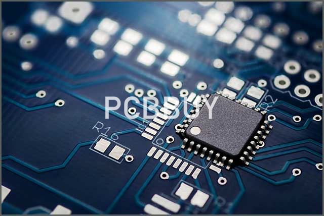
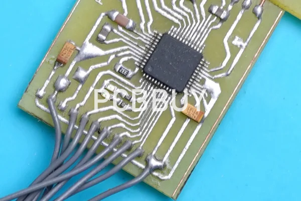
A presensitized circuit board is a special board with a photosensitive surface coating. It enables you to create a customized design by shifting/burning the image with a UV light. In other words, a presensitized circuit board resembles a standard copper-clad board. The only difference between them is how you transfer the design into the boards.
And in this passage, we will lead you to learn the detailed knowledge of presensitized PCB. Come and check the content below.
What are the advantages of presensitized PCB?
Presensitized PCBs have numerous benefits, making them the number one choice of most manufacturers and engineers. Below are the main advantages of presensitized PCBs.
·The main advantage of presensitizing is that it is more accurate than other circuit board processing approaches, like the toner transfer technique.
·The process of presensitization is also very cost-effective. Presensitization excludes fabrication steps, lowering expenses. Therefore, you can experiment with your creative concepts without distressing about going beyond your budget limits.
·Presensitized circuit boards are dense, minimizing the use of several wires on a board. They use interconnections to link parts via copper tracks, unlike the use of multiple cables to conduct current in traditional circuit boards. With presensitized circuit boards, the interconnections are somewhat less immense.
·Presensitized circuit boards are easy to repair in case they break down. Additionally, they are easy to examine and consequently replace individual failure components. This is because manufacturers design and label the electronic parts and polarities present in presensitized boards accurately.

·Presensitized PCBs also save much time during assembling. You will take more time to connect components in traditional PCBs. On the other hand, you will take less time to connect components of presensitized PCBs. This is why many engineers love them.
·Most presensitized boards are resistant to movement. If you are a keen individual, you will realize that most presensitized circuit board components contain strong grips. They employ solders, which limit their movement regardless of the direction of the PCB to achieve stability.
·Presensitized PCBs are highly reliable compared to traditional PCBs. Talking about reliability and performance, presensitized boards provide desirable results. This is also another reason why most electrical engineers choose them over their traditional counterparts.
How to make presensitized PCB?
Here are the steps of making presensitized PCB:
1. PCB Artwork
Remember to scrutinize your tracing paper before utilizing it. Light up one part of the paper with a shiny source of light, and examine it by viewing through the other side. The paper should be free from dark spots and stains. Dark spots cover the artwork portions, forming short circulating pathways around crowded sections of the board artwork.
2. PCB Printing
You should use laser-made positive artwork in your PCB printing exercise as they form delicate, crisps, and compact black prints. Inkjet inks seam to stain with tracing paper, resulting in prints with draining and blurry edges. Consequently, this limits the feasible spacing between circuit board pads and traces.
3. PCB Preparation
It is essential to realize that a presensitized board surface is shielded with a dense grey layer against unintended exposure and impurities. You will use the extended part later to attach your PCB standoff clip during the design and etching process. Burrs and uneven edges may limit your artwork from lying ideally uniform.
4. PCB Exposure
First, clean your exposure box surface with a cloth containing a mild detergent. Then, rinse it with a clean, dry cloth. Take out the protective PCB layer. Thirdly, gently slide your board in between the upper and lower artwork. Fourthly, insert the board in the exposure box. Expose Your PCB for 8 Minutes then fit the Standoffs, finally drip the PCB in Developer Medium.
5. PCB Etching
PCB etching is an important step in the chemical preparation of presensitized PCBs. It involves the removal of copper to obtain desirable patterns. Remember, you need to do away with every copper residue apart from the circuitry covered by the tin plating.
PCB etching seems to be a complicated process for some people, but actually, it is not a challenging activity, as you may think. After collecting all the necessary materials, print your layout before printing the circuit layout. Sketch your design in transparent acetate material to achieve the desired results.
Use a laser printer instead of an inkjet printer to print your acetate. We prefer printed ink on acetate because it does not stick; hence, you will not get undesired results. Alternatively, you can use a laser printer toner. But if you do not have a laser printer, you can make good use of an acetate photocopy.
It would be best to dissolve a developer powder in warm water to form a universal circuit board developer. Most etching agents, like ferric chloride, come in powder or solution form. In the case of dust, apply the same approach with the developer powder.
Industry Category


