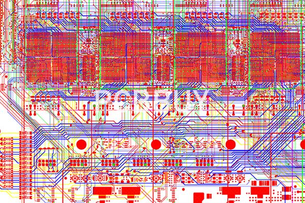
Signal integrity in PCB
By:PCBBUY 06/09/2021 17:32

Signal Integrity (SI) signifies the signal’s ability to propagate without distortion. Signal integrity is nothing but the quality of the signal passing through a transmission line. It gives the measurement of the amount of signal degradation when the signal travels from the driver to the receiver. In the high-frequency regime, both digital and analog aspects of the signal need to be taken care of.
When a signal propagates from the driver to the receiver, it doesn’t remain the same, whatever has been sent originally will be received with varying degrees of distortion. This signal distortion happens due to factors like impedance mismatch, reflections, ringing, crosstalk, jitter, and ground bounce. A designer’s primary aim should be minimizing such factors so that the original signal could make it to the destination with minimum distortion. Special care is also needed to maintain signal quality and to control their undesirable effects in electronic circuitry.
What are the signal integrity issues in PCB?
Frequency
At low frequencies, you should not experience any major problems with signal integrity. However, with increasing signal speeds, you get higher frequencies, which can affect both the analog and digital properties of the system. You may experience reflections, ground bounce, crosstalk and ringing at higher frequencies, which can seriously damage the integrity of your signal.
If you anticipate higher frequencies, you need to consider transmission line effects on the I/O signaling in your PCB board design.
Speed
Naturally, the relationship between speed and frequency is one you need to keep in mind. Lower speeds mean lower frequencies and fewer signal transmission problems, while faster speeds mean higher frequencies and the attendant problems that can come with them.
Length
Another issue to consider when it comes to transmission and signal integrity is the length of the transmission medium. The longer the transmission medium, the greater the chance there’s some type of signal loss.
Fortunately, these and most other signal integrity issues can be counteracted by a quality design and by keeping some basic layout guidelines in mind when designing your printed circuit boards.
What are main signal integrity PCB considerations?
Extensive research has been done on the best way to design transmission lines so high-speed signals can travel at maximum efficiency. To reduce potential problems with signal integrity and other transmission issues, it’s important to make sure your PCB supplier provides boards with a strong design.
Below are some of the guidelines that have been published by many different sources, such as Texas Instruments, that address high-speed signals such as clock signals and their routing and give designers a review of the important coherences. Because many things can affect transmission lines, EMI problems can occur. In order to reduce these problems, good PCB design is important — and with some simple design rules, the PCB designer can minimize these problems.

When approaching your PCBs, the designer should start by asking a few basic questions, including:
·Are there sensitive signals and will those sensitive signals require a stripline, or are a micro strip sufficient?
·How high is the frequency and how fast can the system get?
·What are the electrical specs at sinks and source inputs and outputs?
·How many different supply voltages are there and do they each need their own power plane?
·What are the minimum widths, separations and heights for the traces and what is the minimum distance between layers?
·Are there interconnections between at least two independent functional groups?
·What are the via requirements? Are blind and or buried vias possible?
What are PCB Signal Integrity tips?
Here are a few other tips to keep in mind when it comes to the design of efficient printed circuit boards:
Right angles: Avoid right angles in your traces because they increase capacitance in that region, leading to impedance changes and reflections. 45-degree angles are better and round bends are ideal.
Vias: Although vias can be vitally important to routings, they add inductance and capacitance and lead to reflections. They also increase trace length, so use them sparingly and avoid vias in differential traces.
Signal Separation: Keep your high-speed and low-speed signals apart from each other. Separate your digital and analog signals as well. Route signals 90 degrees to each other to minimize crosstalk.
Industry Category


